A Trustworthy PCB and Electronic Manufacturing Enterprise! Contact Us


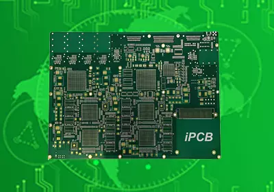

Product: 6-layer circuit board
Material: FR-4 (Grade A, Tg 130-170°C); Optional high-frequency substrates (e.g., Rogers) for RF applications; Green epoxy solder mask (10-15μm thickness)
Quality standard: IPC-6012 (performance specification), IPC-A-610 (acceptability criteria); RoHS 2.0, REACH compliant
Dielectric constant: 4.2-4.7 @ 1MHz (FR-4);
Layers: 6 layers (typically 3 signal layers, 2 power layers, 1 ground layer; configurable based on design)
Thickness: 1.6mm (standard); Customizable 0.8-3.2mm; Tolerance ±0.1mm (for thickness ≥0.8mm)
Copper thickness: Inner layers: 0.5oz (17.5μm); Outer layers: 1oz (35μm); High-power variants: 2-3oz (70-105μm)
Surface technology: ENIG (4-6μm Ni, 0.05-0.1μm Au); Optional HASL (lead-free), OSP (organic solderability preservative)
Special requirements: Minimum line width/spacing: 3-5mil (0.076-0.127μm);
Application: Industrial control (PLCs, automation modules)
When engineers face "wiring congestion," "signal interference," and "space constraints" in high-complexity devices—from industrial PLCs to 5G base stations and medical ultrasound machines—the 6-layer circuit board emerges as a game-changer. Unlike 4-layer or 2-layer PCBs, its scientific lamination design (typical structure: Signal/Ground/Power/Signal/Ground/Signal) adds 2 extra power/ground planes, cutting electromagnetic interference (EMI) by up to 70% while compressing intricate circuits into compact spaces—critical for miniaturized, high-performance electronics.
6-layer circuit board
Core Advantages Backed by Professional Specifications
Crafted to meet industrial-grade reliability and precision demands, this 6-layer PCB stands out with tailored technical details:
Base Material & Thermal Stability: Adopts Grade A FR-4 (Tg 130–170°C) for general scenarios; optional Rogers high-frequency substrates (e.g., RO4350B) for 5G RF modules, ensuring dielectric constant stability (4.2–4.7 @ 1MHz for FR-4, 3.0–3.5 @ 10GHz for Rogers).
Lamination & Wiring Density: 6 layers with 3 independent signal layers, 2 power layers, and 1 ground layer; supports blind/buried vias (reducing 50% surface hole occupancy) and minimum line width/spacing of 3mil (0.076mm)—ideal for FPGA/CPU with 1000+ pins.
Copper Thickness & Surface Finish: Inner layers (0.5oz/17.5μm) for low-power signal transmission; outer layers (1–3oz/35–105μm) for high-current scenarios (e.g., automotive ECUs); ENIG finish (4–6μm Ni + 0.05–0.1μm Au) as standard, compatible with BGA soldering and 500+ insertion cycles.
Impedance Control: 50Ω (single-ended) / 100Ω (differential pair) ±10%, matching PCIe 4.0, DDR5, and 5G NR protocols—critical for 10Gbps+ high-speed signal integrity.
Industry-Specific Applications: Solving Real-World Pain Points
This 6-layer circuit board isn’t just a component—it’s a tailored solution for 3 key sectors:
Industrial Automation: Used in semiconductor wafer-cutting equipment’s PLC modules, the dual ground layers reduce signal crosstalk to -45dB, ensuring 24/7 stable operation of motion control systems.
5G Telecom: Integrated into 5G small base station RF processing boards, Rogers substrates and precise impedance control lower insertion loss to ≤-1.2dB, supporting 32GB/s data throughput for massive MIMO technology.
Medical Devices: Applied in portable ultrasound machines, its compact lamination (1.6mm standard thickness) and 168-hour high-temperature aging test (85°C/85% RH) meet medical-grade reliability, enabling clear image transmission without interference.
Authority & Customization Support
Compliant with IPC-6012 (performance), IPC-A-610 (acceptability), RoHS 2.0, and REACH; optional AEC-Q200 certification for automotive electronics.
Need a tailored 6-layer circuit board? Share your device’s power, signal, and space requirements—reach out to the iPCB technical team for a customized solution.
Product: 6-layer circuit board
Material: FR-4 (Grade A, Tg 130-170°C); Optional high-frequency substrates (e.g., Rogers) for RF applications; Green epoxy solder mask (10-15μm thickness)
Quality standard: IPC-6012 (performance specification), IPC-A-610 (acceptability criteria); RoHS 2.0, REACH compliant
Dielectric constant: 4.2-4.7 @ 1MHz (FR-4);
Layers: 6 layers (typically 3 signal layers, 2 power layers, 1 ground layer; configurable based on design)
Thickness: 1.6mm (standard); Customizable 0.8-3.2mm; Tolerance ±0.1mm (for thickness ≥0.8mm)
Copper thickness: Inner layers: 0.5oz (17.5μm); Outer layers: 1oz (35μm); High-power variants: 2-3oz (70-105μm)
Surface technology: ENIG (4-6μm Ni, 0.05-0.1μm Au); Optional HASL (lead-free), OSP (organic solderability preservative)
Special requirements: Minimum line width/spacing: 3-5mil (0.076-0.127μm);
Application: Industrial control (PLCs, automation modules)
iPCB Circuit provides support for PCB design, PCB technology, and PCBA assembly. You can request technical consultation or quotation for PCB and PCBA here, please contact email: sales@ipcb.com
We will respond very quickly.
