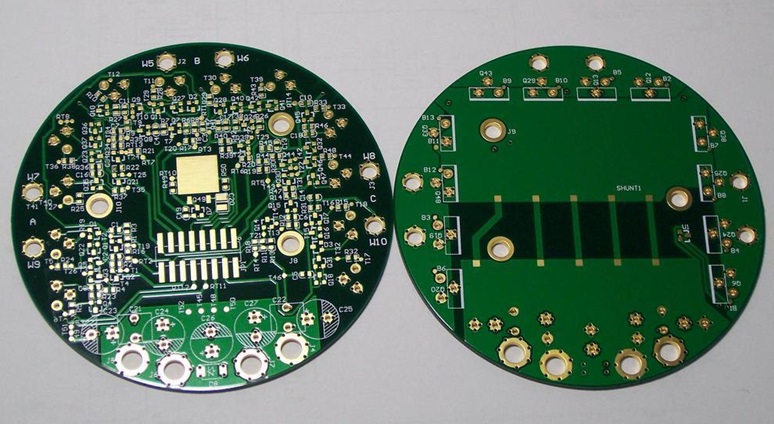
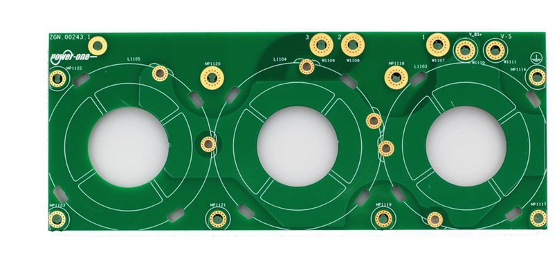
Printed circuit boards come in a variety of shapes, including octagonal, circular, rectangular, and other unusual shapes. However, the most common shapes are square and rectangular PCBs. Round PCB boards are less common than rectangular PCBs. However, as electronic products become smaller, smarter, and more aesthetically pleasing, the demand for round PCB boards is growing.
Why We Choose Round PCB Boards
Traditional PCBs are mostly rectangular or square because these shapes are easy to design, manufacture, and assemble. However, the pursuit of space efficiency and aesthetic design in many modern electronic devices has prompted engineers to seek more flexible solutions. Round PCB boards have emerged precisely in this context.

round pcb board
Round PCB boards are circuit boards with a circular or nearly circular design. Circular PCBs are not simply aesthetically pleasing; they offer unique advantages in many practical applications:
-Space Optimization: In round or irregularly shaped housings, round PCB boards maximize internal space utilization, eliminating dead space and enabling more compact product designs. For example, smartwatches, circular displays, LED lamps, and certain medical devices all benefit from their shape.
-Structural Integration: Round PCB boards can better integrate with circular mechanical structures or rotating components, simplifying the overall assembly process.
-Signal Integrity: In certain high-frequency applications, a circular layout helps optimize signal paths, reducing edge effects and thus improving signal integrity.
-Excellent Heat Dissipation: Their structural design helps improve heat dissipation, making them particularly suitable for high-power applications such as LED lighting.
These unique advantages make round PCB boards stand out among many electronic product manufacturers, making them an essential tool for designers to solve specific challenges.
Design Challenges and Solutions for Circular PCBs
While round PCB boards offer many advantages, their design process is also more complex than traditional rectangular PCBs. The following are some key challenges and their corresponding solutions:
1. Layout and Routing Complexity
Circular edges restrict component placement and routing. Components often need to be arranged along curved lines or radiate from the center, making them difficult for automated routing tools to optimize and significantly increasing the workload for manual routing. Separating power and ground planes, as well as isolating signal lines, are also more challenging in circular layouts.
Solutions:
-Sector Division: Divide a circular board into multiple sectors, each responsible for a specific functional module, and then organically connect these modules.
-Centrosymmetric Layout: For certain applications, adopting a centrosymmetric layout can simplify routing and improve heat dissipation and signal balance.
-Multi-layer Design: Increasing the number of layers is an effective way to address routing density. Using more layers to distribute signals, power, and ground effectively alleviates routing pressure in circular layouts.
-Advanced EDA Tools: Choose EDA software that supports custom-shaped boards, such as Altium Designer, Cadence Allegro, and Siemens EDA. Take advantage of advanced routing features, such as teardrop connections and differential pair routing.
-Pre-Planning: Detailed planning of key component placement and primary signal flow is crucial early in the design process to minimize late-stage modifications.
2. Component Selection and Package
Within a limited circular space, choosing the appropriate component package type is crucial. Especially for large or irregularly shaped components, their placement requires careful consideration to avoid interfering with other components or extending beyond the board edges.
Solution:
Preferably use small, low-profile surface-mount devices (SMDs), such as resistors and capacitors in 0201 and 0402 packages, and chips in QFN and BGA packages. In extreme cases, it may be necessary to work with the supplier to customize specialized packages. Also, ensure proper layout. Place the core chip in the center, then arrange smaller passive components and connectors toward the periphery. Ensure adequate space for heat dissipation components.

round pcb board
3. Signal Integrity and Power Integrity
In a circular board, trace lengths and paths may be irregular, which can lead to signal reflections, crosstalk, and electromagnetic interference (EMI) issues. The power and ground plane design may also have discontinuities due to the shape, compromising power integrity.
Solution:
-Equal-length routing: For high-speed signal lines, maintain equal routing lengths to minimize timing skew. Differential Pair Routing: For high-speed differential signals, use tightly coupled differential pair routing and ensure impedance matching.
-Complete Ground Plane: Maintain the integrity of the ground plane as much as possible and avoid excessive splits, especially under high-speed signal areas. If splits are necessary, ensure adequate via connections.
-Decoupling Capacitors: Place sufficient decoupling capacitors near the chip power pins to filter out high-frequency noise.
-Impedance Control: Work closely with the PCB manufacturer to ensure that the transmission line impedance on round PCB boards meets design requirements.
4. Thermal Management
The relatively small edge area of a round PCB board may limit heat dissipation. Heat buildup is a common problem in compact circular enclosures.
Solution:
-Thermal Path: Provide a large area of copper foil under heat-generating components as a heat dissipation path and connect to other layers through thermal vias.
-Heat Sink: Consider using a small heat sink or thermal pad for high-power devices.
-Thermal Simulation: Use thermal simulation software to perform thermal analysis on round PCB boards to predict hot spots and optimize component placement. Housing design: Consider adding heat dissipation holes or using a metal housing for heat dissipation in combination with the product housing design.
5. Manufacturing and Testing
The manufacturing process for round PCB boards, particularly cutting, drilling, and assembly, can be more complex than for traditional rectangular boards. Test fixtures also need to be designed to accommodate the round shape.
Solutions:
High-Precision Machining: Select a PCB manufacturer with high-precision CNC milling and drilling capabilities.
Custom Fixtures: Design custom test fixtures and assembly tools for round PCBs.
Design for Manufacturability (DFM): Consider manufacturability during the design phase and communicate with the manufacturer to understand their process capabilities and limitations.
Facing these design challenges, experienced engineers need to utilize specialized EDA tools, combine extensive practical experience, and collaborate closely with the PCB manufacturer to successfully develop high-performance round PCB boards.
Conclusion:
Round PCB boards, as a specialized circuit board format, demonstrate tremendous potential in a wide range of fields, including smartwatches, LED lighting, and medical devices, thanks to their unique shape. While their design and manufacturing processes present numerous challenges, these are being gradually overcome with the continuous advancement of technology and the increasing sophistication of manufacturing processes. From the initial design concept to rigorous layout and routing, and finally to precise manufacturing and testing, every step is crucial to the performance and reliability of the final product.