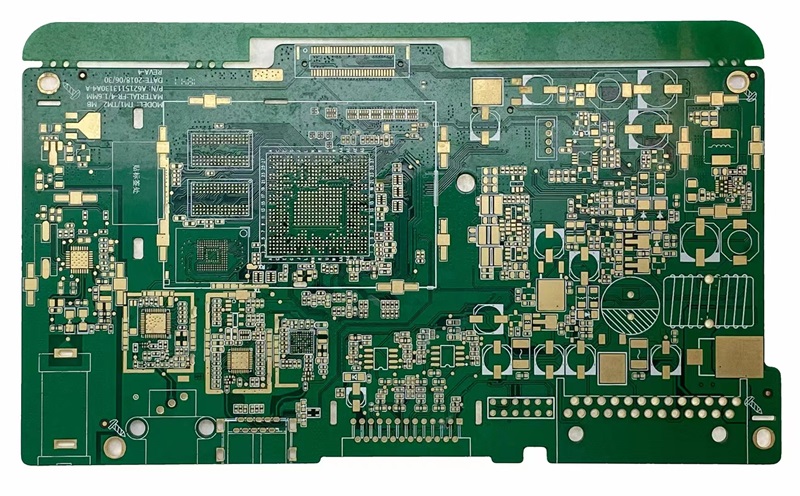
In the early days of electronics, circuit boards were simple, single-layered pieces of material. However, as our gadgets became smaller, faster, and more powerful, the internal architecture had to evolve. Today, the backbone of almost every advanced device, from the smartphone in your pocket to the satellite orbiting Earth, is the multilayer pcb board. By stacking multiple layers of conductive and insulating materials, engineers can cram incredible amounts of computing power into tiny footprints. In this guide, we will explore why this technology is the gold standard for modern hardware.

multilayer pcb board
What Exactly is a Multilayer PCB Board?
At its simplest, a multilayer pcb board is a circuit board that has three or more layers of conductive copper foil. Imagine a sandwich where the bread slices are insulating substrate materials (like FR-4) and the fillings are thin sheets of copper. These layers are laminated together under high heat and pressure to create a single, rigid structure.
Unlike double-sided boards, which only have circuitry on the top and bottom, a multilayer design utilizes internal layers for power distribution and complex signal routing. These layers are connected through specialized vertical holes called "vias."
Key Advantages for High-Performance Designs
Why do manufacturers choose a multilayer pcb board instead of a cheaper single-layer alternative? The answer lies in performance and physics.
Miniaturization: By using the vertical dimension, designers can reduce the overall surface area of the board. This is why a modern laptop can be thinner than a book but a thousand times more powerful than the room-sized computers of the past.
Enhanced Signal Integrity: High-speed circuits are prone to electromagnetic interference (EMI). In a multilayer design, internal layers can act as "ground planes" or "power planes." These planes provide a shield that prevents noise from interfering with sensitive signals, ensuring that your device operates reliably without crashes.
Durability and Quality: These boards are built to last. The lamination process results in a very sturdy product that can withstand more physical stress and heat than simpler boards.
The Complex Manufacturing Process
Creating a multilayer pcb board is a feat of precision engineering. It starts with the inner layers, which are etched with their circuit patterns first. Once the inner layers are ready, they are stacked with "prepreg" (an insulating material infused with resin) and copper foil.
One of the most critical aspects of this process is the drilling of vias. In advanced boards, manufacturers use Blind Vias (which connect an outer layer to an inner layer) and Buried Vias (which connect two inner layers without being visible from the outside). This allows for even higher density because the outer surface remains clear for mounting microscopic components. Finally, the entire stack is pressed in a hydraulic machine to ensure there are no air bubbles, which could cause the board to fail under high temperatures.
Common Applications in Industry
You will find these boards in environments where failure is not an option.
Medical Equipment: High-resolution imaging machines (like MRIs) and heart monitors require the extreme precision that only multilayer technology can provide.
Aerospace: Satellites and aircraft controls must be lightweight yet incredibly robust to survive extreme vibrations and temperature shifts.
Consumer Tech: Your laptop, gaming console, and smart home hub all rely on 4-layer to 12-layer boards to manage high-speed data processing.
How to Choose the Right Number of Layers?
When designing a product, cost is always a factor. A 4-layer board is the most common starting point for professional electronics, offering a good balance between cost and EMI protection. However, as the complexity of the chips (like CPUs or FPGAs) increases, you may need an 8, 10, or even 32-layer stack-up. The key is to work with a manufacturer who understands impedance control—ensuring the signals move at the correct speed through the copper traces.
Conclusion
As we push the boundaries of Artificial Intelligence, 5G, and IoT, the demand for sophisticated circuitry will only grow. The multilayer pcb board has proven to be an essential tool in this digital revolution, offering the density, speed, and reliability that modern consumers demand. By understanding the layers beneath the surface, businesses can make better-informed decisions about their hardware development, ensuring their products are built on a foundation of quality and innovation.