A Trustworthy PCB and Electronic Manufacturing Enterprise! Contact Us


To make a fantastic assembly prototype, you need to know
1. What is a schematic diagram?
2. What is a package?
3. How does a schematic diagram become a PCB?
4. How does a PCB ultimately become a circuit board?
5. What is SMT?
First, let's talk about the concept of a schematic diagram: a diagram showing the connection principles between various components on a circuit board.
In other words, any diagram that reflects the circuit principles is a schematic diagram.
Whether hand-drawn or computer-generated, as long as it allows readers to understand the circuit principles, it qualifies.
What are circuit principles?
For example:
Why does the LED on the circuit board light up? We all know that as long as power is applied to the LED, it will light up.
This is a fact we all know. But what if we know nothing?
If you are given a new circuit board, how should it function? What is the underlying principle?

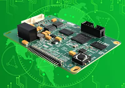
assembly prototype
How do you repair it if something goes wrong?
This is what a schematic diagram does—it describes the operational process of the circuit system.
Hand-drawn schematic diagrams:
Drawing schematic diagrams using software
What is packaging? What is packaging?
Packaging refers to connecting the circuit pins on a silicon wafer to external terminals via wires to enable connection with other components. The packaging form refers to the housing used to install semiconductor integrated circuit chips. It not only serves to install, secure, seal, protect the chip, and enhance electrical and thermal performance, but also connects the chip's contacts to the pins on the package housing via wires. These pins are then connected to other components via wires on the printed circuit board, thereby achieving connectivity between the internal chip and external circuits.
The size of the pad and the spacing between pads are referred to as the resistor's package.
In other words, finding a suitable location on the circuit board to properly install the resistor or other components, this suitable location is referred to as the package.
Schematic diagrams are used to describe the principles of the entire system circuit, while packages provide installation locations for components on the PCB.
Have you ever thought about it?
After the circuit schematic diagram is completed, how do you map the components on the schematic diagram to the component packages on the PCB?
This is the role of the circuit schematic diagram!
The purpose is to systematically link the packages of all components on the PCB together to ensure the circuit functions properly.
What is this ‘systematic’ approach? It follows the connections in the schematic diagram!
Step one: First, you need to draw the schematic diagram, right?
Step two: After adding packages to the components according to the connection rules in the schematic diagram, generate the PCB. At this point, you can see the electrical connections on the PCB.
Step 3: Refer to the electrical connections in the schematic diagram to complete the PCB layout.
After completing the PCB layout, you can view the PCB preview.

assembly prototype
What is SMT?
SMT: Surface Mount Technology (SMT) is the most widely used technology and process in the electronics assembly industry.
It involves installing leadless or short-lead surface-mount components (abbreviated as SMC/SMD, also known as chip components) on the surface of a printed circuit board (PCB) or other substrate, and then assembling them through processes such as reflow soldering or wave soldering.
In other words, there are specialised machines to complete the component installation and soldering process, eliminating the need for manual labour.
The benefits of a one-stop service:
For companies: If you need to produce circuit boards yourself, you will inevitably need to establish some key positions. By using iPCB's one-stop service, you can save on personnel costs and allow professionals to focus on their specialised tasks.
Procurement: You no longer need to manage those small, scattered parts.
Technology: You can allocate more time to verifying solutions.
After designing, you can give us your assembly prototype, and we will make it come true.