A Trustworthy PCB and Electronic Manufacturing Enterprise! Contact Us


Product: Black Solder Mask PCB
Material: FR-4 substrate (A-grade, optional high-Tg variant with Tg 165–180°C for high-temperature scenarios);
Black solder mask: Custom-formulated epoxy-based UV/thermal-curable ink
Quality standard: IPC-6012
Dielectric constant: FR-4 substrate: 4.3–4.7 @ 1MHz–1GHz; Black solder mask: 3.6–4.4 @ 1MHz (standard ink), 3.1–3.4 @ 1GHz (high-frequency optimized ink)
Layers: 1–24 layers (typical: 4–6 layers for consumer electronics; 8–16 layers for industrial/automotive applications)
Thickness: Substrate: 0.5–6.0mm; Overall board: 0.8–7.5mm (varies by layer count); Tolerance: ±0.08mm (for thickness ≥0.8mm)
Copper thickness: Inner layers: 0.5–2oz (17–70μm); Outer layers: 1–3oz (35–105μm)
Surface technology: ENIG (Electroless Nickel Immersion Gold) – Nickel layer: 4.5–5.5μm (phosphorus content 8%±0.5%); Gold layer: 0.06–0.09μm; Black solder mask thickness: 12–15μm (UV/thermal cured)
Special requirements: High-Tg substrate (Tg 165–180°C) required for -40°C~125°C operating environments; Storage: 23±2°C, 45%–55% humidity (vacuum-packed to prevent sulfur contamination of ENIG finish); Minimum line width/spacing: 4/4mil (0.1016/0.1016mm) with advanced laser direct imaging
Application: High-end consumer electronics (flagship smartphone RF boards, smart wearable devices, gaming console modules); Industrial/automotive (ADAS sensors, 5G small cell PCBs); Medical (diagnostic equipment signal-processing boards)
In the competitive landscape of mid-to-high-end electronics—from flagship smartphones to medical diagnostic gear—Black Solder Mask PCB stands out as a dual-duty solution: it delivers a sleek, professional aesthetic that elevates product design, while packing industrial-grade performance to meet strict signal integrity, corrosion resistance, and temperature demands. Built on optimized FR-4 substrates and precision manufacturing, this PCB is engineered to solve the unique challenges of modern electronics, where "looks" and "function" can’t be compromised.
Sleek Aesthetics + Robust Protection: The Black Solder Mask Advantage
Unlike standard colored PCBs, the black solder mask of this ENIG Black Solder Mask PCB isn’t just about visual appeal—it’s a protective barrier tailored for durability. We use custom-formulated epoxy-based UV/thermal-curable ink, applied to a thickness of 12–15μm, to shield copper traces from oxidation, moisture, and mechanical wear. This design not only prevents solder shorts during assembly but also hides minor surface imperfections, making it the top choice for consumer electronics brands aiming for a premium, seamless look (think flagship smartphone RF boards or high-end smart wearable devices).
Paired with ENIG (Electroless Nickel Immersion Gold) surface technology—featuring a 4.5–5.5μm nickel layer (with 8%±0.5% phosphorus for anti-corrosion) and 0.06–0.09μm gold layer—the high-precision Black Solder Mask PCB ensures exceptional conductivity and solderability. This combo is critical for fine-pitch components like BGAs or high-speed ICs, common in gaming console modules and 5G small cell PCBs, where reliable connections directly impact performance.
Performance Tuned for Every Scenario: From Temperature to Signal
We’ve optimized the Black Solder Mask PCB to adapt to diverse application needs, starting with its core materials and parameters—making it a top pick for automotive ADAS PCB and medical diagnostic equipment PCB projects:
High-Temperature Resilience: Choose the optional high-Tg Black Solder Mask PCB (Tg 165–180°C) for environments ranging from -40°C to 125°C—perfect for automotive ADAS sensors or industrial control modules that face extreme temperature fluctuations. Even standard A-grade FR-4 handles routine soldering and indoor use with ease.
Stable Signal Integrity: The FR-4 substrate boasts a dielectric constant of 4.3–4.7 @ 1MHz–1GHz, while high-frequency optimized black ink (3.1–3.4 @ 1GHz) minimizes signal loss. This makes the PCB ideal for RF boards in smartphones or signal-processing units in medical diagnostic equipment, where signal accuracy is non-negotiable.
Flexible Layer & Copper Options: With 1–24 layers (4–6 layers for consumer tech, 8–16 layers for industrial/automotive use) and copper thicknesses of 0.5–2oz (inner layers) and 1–3oz (outer layers), this multi-layer Black Solder Mask PCB balances power handling and miniaturization. Whether you need to power a small wearable (0.5oz copper) or an ADAS sensor (3oz outer copper), the design scales without compromise.
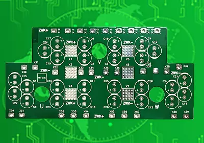
Black solder mask PCB
Trusted by Key Industries: Where Reliability Matters Most
The Black Solder Mask PCB isn’t just a component—it’s a trusted partner across high-stakes sectors, aligning with needs for high-end consumer electronics PCB and industrial control PCB:
High-End Consumer Electronics: Powers flagship smartphone RF boards, smart wearable devices, and gaming console modules, blending premium looks with consistent performance.
Industrial & Automotive: Supports ADAS sensors and 5G small cell PCBs, withstanding vibration, temperature shifts, and harsh operating conditions thanks to its high-Tg substrate and ENIG finish.
Medical Technology: Used in diagnostic equipment signal-processing boards, where corrosion resistance (from ENIG) and stable signal integrity (from optimized dielectric properties) meet strict regulatory standards.
Every PCB meets global quality benchmarks: IPC-6012 (PCB performance), IPC-4552B (ENIG specs), UL94 V-0 flame retardancy, and RoHS 2.0/REACH compliance—so you can integrate with confidence.
Ready to Customize? Connect with the IPCB Technical Team
No two projects are the same—and your Black Solder Mask PCB shouldn’t be either. Whether you need to tweak layer counts, upgrade to high-Tg substrates for extreme temperatures, or optimize line width/spacing to 4/4mil (0.1016/0.1016mm) via laser direct imaging, the IPCB technical team has the expertise to tailor the PCB to your exact needs. We’ll guide you from material selection to mass production, ensuring your design meets performance goals and timeline.
Reach out to the IPCB technical team today to discuss your Black Solder Mask PCB project—let’s build an electronics solution that looks as good as it performs.
Product: Black Solder Mask PCB
Material: FR-4 substrate (A-grade, optional high-Tg variant with Tg 165–180°C for high-temperature scenarios);
Black solder mask: Custom-formulated epoxy-based UV/thermal-curable ink
Quality standard: IPC-6012
Dielectric constant: FR-4 substrate: 4.3–4.7 @ 1MHz–1GHz; Black solder mask: 3.6–4.4 @ 1MHz (standard ink), 3.1–3.4 @ 1GHz (high-frequency optimized ink)
Layers: 1–24 layers (typical: 4–6 layers for consumer electronics; 8–16 layers for industrial/automotive applications)
Thickness: Substrate: 0.5–6.0mm; Overall board: 0.8–7.5mm (varies by layer count); Tolerance: ±0.08mm (for thickness ≥0.8mm)
Copper thickness: Inner layers: 0.5–2oz (17–70μm); Outer layers: 1–3oz (35–105μm)
Surface technology: ENIG (Electroless Nickel Immersion Gold) – Nickel layer: 4.5–5.5μm (phosphorus content 8%±0.5%); Gold layer: 0.06–0.09μm; Black solder mask thickness: 12–15μm (UV/thermal cured)
Special requirements: High-Tg substrate (Tg 165–180°C) required for -40°C~125°C operating environments; Storage: 23±2°C, 45%–55% humidity (vacuum-packed to prevent sulfur contamination of ENIG finish); Minimum line width/spacing: 4/4mil (0.1016/0.1016mm) with advanced laser direct imaging
Application: High-end consumer electronics (flagship smartphone RF boards, smart wearable devices, gaming console modules); Industrial/automotive (ADAS sensors, 5G small cell PCBs); Medical (diagnostic equipment signal-processing boards)
iPCB Circuit provides support for PCB design, PCB technology, and PCBA assembly. You can request technical consultation or quotation for PCB and PCBA here, please contact email: sales@ipcb.com
We will respond very quickly.
