A Trustworthy PCB and Electronic Manufacturing Enterprise! Contact Us


In the electronics industry, capacitive sensors are widely used in modern electronics for touch, proximity, and motion detection, offering precise and contactless control. In PCB manufacturing, their performance relies heavily on board design and material quality. The PCB not only carries the sensing electrodes but also determines field stability, noise resistance, and sensitivity. This article focuses on how PCB design, materials, and fabrication processes impact the efficiency and accuracy of capacitive sensors in electronic devices.

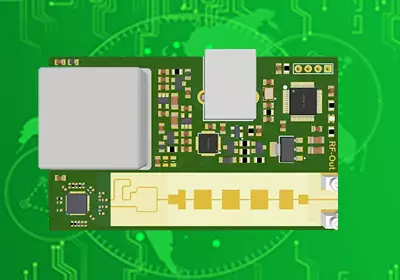
capacitive sensor
1. PCB Design Principles for Capacitive Sensors
1.1 Electrode Pattern Design
The electrode pattern is the foundation of every capacitive sensor PCB. The geometry—whether circular, rectangular, or interdigitated—determines how the electric field distributes across the sensing area. Interdigitated (finger-like) patterns are commonly used for higher sensitivity, as they increase the effective electrode area without enlarging the board.
Designers must carefully balance electrode size and spacing. Larger electrodes increase base capacitance and sensitivity but also make the system more prone to environmental noise. On the other hand, smaller electrodes offer higher resolution but lower detection range. Consistency in electrode symmetry ensures stable signal behavior and reduces parasitic effects during manufacturing.
1.2 Layer Stack-Up and Structure
In multilayer PCB designs, capacitive sensors usually consist of three main layers: the sensing layer, a shielding layer, and a controller layer.
---The sensing layer holds the electrodes that detect touch or proximity.
---The shielding layer isolates the sensing layer from noise sources and ground planes.
---The controller layer connects the signal routing to the processing circuit or microcontroller.
Proper layer stack-up allows stable capacitance readings while reducing interference from power traces or nearby signals. PCB designers often use driven shields—connected to a reference voltage that follows the sensor signal—to minimize parasitic capacitance and external coupling.
1.3 Routing Rules and Grounding
Signal routing is critical in ensuring high signal-to-noise ratio (SNR). Since capacitive sensing relies on very small capacitance changes (in the femtofarad range), long traces can introduce unwanted parasitic effects. The routing between the sensor electrode and the controller IC should be as short and direct as possible.
Ground planes should be placed strategically: too close to the sensing area may reduce sensitivity, but without proper grounding, environmental noise can dominate. A guard ring—a grounded trace surrounding the sensor electrode—helps stabilize the electric field and provides a barrier against stray capacitance.
2. Manufacturing and Fabrication Process
2.1 Copper Etching and Pattern Precision
Accurate copper patterning is essential for reliable capacitive sensors. Fine line width and spacing determine the exact shape of the electric field. Advanced etching and laser direct imaging (LDI) technology ensure consistent electrode geometry and minimal misalignment.
For high-density sensors, copper thickness should be uniform (typically 18–35 μm) to maintain even electric fields. Variations in plating thickness can shift capacitance values, leading to unstable sensor outputs.
2.2 Layer Registration and Lamination
Multilayer capacitive sensor PCBs require precise registration between layers to align electrodes accurately. Even a small offset during lamination can distort the electric field and alter sensitivity. Manufacturers use optical alignment and controlled lamination pressure to keep tolerances within ±25 μm.
The dielectric thickness between the sensor and shield layers must also remain consistent. Uneven lamination may lead to sensitivity differences across keys or touch zones.
2.3 Surface Finishing and Protective Coatings
Surface finishes like ENIG (Electroless Nickel Immersion Gold), OSP, or immersion tin protect copper electrodes from oxidation. However, the choice of finish also affects capacitance—gold finishes tend to add slight parasitic capacitance due to higher permittivity.
For outdoor or industrial environments, conformal coating or waterproof layers (such as silicone or polyurethane) can protect the board while maintaining sensor functionality. The coating thickness should be controlled to avoid excessive capacitance drift.
3. Design Challenges and Optimization Strategies
Designing a capacitive sensor PCB involves balancing sensitivity, stability, and manufacturability.
---EMI and Crosstalk: Sensitive analog traces should be separated from digital or high-current paths.
---Ground Shield Optimization: Incorrectly grounded shields can reduce sensitivity instead of improving it.
---Moisture Sensitivity: FR-4 can absorb moisture, slightly altering dielectric properties. Protective coating and compensation circuits help mitigate this effect.
---Environmental Drift: Temperature or humidity compensation algorithms are essential in industrial environments.
---Miniaturization: As devices become thinner, engineers use thinner dielectrics and finer trace widths to maintain sensitivity without increasing area.
4. Conclusion
As capacitive sensors advance, PCB technology remains key to their accuracy and stability. Every stage—from electrode design to lamination—impacts performance. Using quality materials and precise fabrication enables PCBs that a
re more reliable, sensitive, and ideal for modern smart systems.