A Trustworthy PCB and Electronic Manufacturing Enterprise! Contact Us


Product: IC Substrate
Material:
Core: BT resin (Tg≥181℃, CTE 13.5–16.5 ppm/℃); ABF (Tg≥183℃, CTE≤9.7 ppm/℃); Ceramic (AlN: 138–177 W/(m·K), Si₃N₄: ≥790 MPa)
Prepreg: HL832-NX, MCL-E-679 series, thickness 24–39 μm
Quality standard: IPC-4101F, IEC 249-2, AEC-Q200, UL94 V-0
Dielectric constant:
BT resin: 4.05–4.15@1MHz; ABF: 3.47±0.1@1GHz; Si₃N₄: 3.77±0.1@10GHz
Layers: Standard 2–13 layers (WB-BGA/CSP); High-density 6–21 layers (FC-BGA)
Thickness:
Substrate: 0.12–3.1 mm; Build-up dielectric: 24–39 μm
Copper thickness:
Signal layer: 11–34 μm; Core layer: 24 μm (typical); Build-up layer: 17 μm (nominal)
Surface technology:
Primary: ENEPIG (Ni 2.9–4.9 μm / Pd 0.09–0.24 μm / Au 0.04–0.09 μm)
Options: OSP (0.14–0.39 μm), Immersion Tin (1.1–2.4 μm)
Special requirements:
Min line/space: 8/11 μm; Microvia diameter: 58–141 μm
Warpage ≤0.72%; Thermal cycle (-54℃~151℃, 1050 cycles no delamination)
Application:
HPC: CPU/GPU (FC-BGA); Consumer: Mobile AP (CSP); Automotive: ADAS radar; 5G: RF modules
For electronics that operate where heat, vibration, or extreme temperatures destroy ordinary PCBs—Ceramic PCB is the uncompromising solution. Unlike FR-4 or organic substrates, it leverages ceramic’s inherent thermal conductivity and mechanical toughness to keep high-power, high-frequency devices running reliably—whether in the heat of an EV inverter, the vibration of an aerospace sensor, or the high-frequency demands of 5G millimeter-wave antennas.
Built for Heat: The Thermal Advantage That Matters
Ceramic PCB’s biggest edge lies in solving the “overheating crisis” that plagues power and high-performance electronics:
AlN Ceramic PCB: Delivers 138–177 W/(m·K) thermal conductivity—8–12x higher than FR-4—matching the CTE of silicon (≈4.3 ppm/℃) to eliminate thermal stress. It’s the go-to for IGBT modules, laser diodes, and EV powertrains where even 10℃ of excess heat risks failure.
Al₂O₃ Ceramic PCB: Balances performance and cost with 15–24 W/(m・K) thermal conductivity and ≥310 MPa flexural strength. Perfect for high-brightness LED ,consumer electronics, and low-to-medium power industrial drivers.
Si₃N₄ Ceramic PCB: The “tough thermal workhorse” with 62–88 W/(m·K) conductivity and ≥790 MPa strength. It withstands thermal shock (-54℃ to 152℃) and vibration in automotive powertrains, satellite components, and heavy-duty robotics.

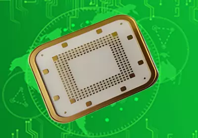
Ceramic PCB
Crafted for Extreme Use: Processes That Boost Reliability
Every detail of our Ceramic PCB is engineered to survive harsh conditions—no shortcuts:
Metalization That Bonds, Not Breaks: Choose DBC (Direct Bonded Copper) (bond strength ≥24 N/mm) for seamless heat transfer in high-power circuits, or AMB (Active Metal Brazing) for hermetic sealing in moisture/dust-prone environments (e.g., industrial inverters). Copper layers are tailored: 5–34 μm for fine RF routing (5G modules) or 67–172 μm for high-current delivery (solar converters).
Precision for High Frequencies: Laser-drilled microvias (56–140 μm) and impedance control (±4.7%) ensure stable signal transmission in 5G/6G RF modules. Substrate thickness (0.12–3.9 mm) and build-up dielectrics (23–38 μm) adapt to miniaturized designs (e.g., wearable sensors) without sacrificing durability.
Finishes That Last: Primary ENEPIG (Ni 2.9–4.8 μm / Pd 0.09–0.23 μm / Au 0.04–0.08 μm) resists 950+ hours of salt spray—critical for automotive and marine electronics. Optional hard gold (for high-wear contacts) or immersion tin (cost-effective short-term storage) adds flexibility.
Reliability Backed by Standards
This isn’t just a substrate—it’s a promise of performance under pressure:
Withstands 1,050 thermal cycles (-54℃ to 152℃) with no delamination, and operates continuously at up to 290℃.
Warpage ≤0.47% (for boards ≥0.5 mm thick) to fit automated assembly lines, no rework needed.
Meets AEC-Q200 (automotive-grade), IPC-6012F, UL94 V-0, and RoHS 3.0—compliant for global markets from EVs to aerospace.
Where Ceramic PCB Makes the Difference
It’s not just a component—it’s the reason critical systems work when they need to:
Automotive: AEC-Q200 variants power ADAS radar, LiDAR, and EV inverters—keeping electrified/autonomous cars safe in -40℃ winters and 120℃ engine bays.
5G/6G: Low-dielectric-loss Si₃N₄ substrates (Dk 3.77±0.1@10GHz) enable millimeter-wave antennas and RF power amplifiers with minimal signal loss.
Aerospace & Industrial: Si₃N₄ PCB survives satellite launches (vibration + extreme cold), while AlN PCB keeps industrial inverters cool in 50℃ factory floors.
Product: IC Substrate
Material:
Core: BT resin (Tg≥181℃, CTE 13.5–16.5 ppm/℃); ABF (Tg≥183℃, CTE≤9.7 ppm/℃); Ceramic (AlN: 138–177 W/(m·K), Si₃N₄: ≥790 MPa)
Prepreg: HL832-NX, MCL-E-679 series, thickness 24–39 μm
Quality standard: IPC-4101F, IEC 249-2, AEC-Q200, UL94 V-0
Dielectric constant:
BT resin: 4.05–4.15@1MHz; ABF: 3.47±0.1@1GHz; Si₃N₄: 3.77±0.1@10GHz
Layers: Standard 2–13 layers (WB-BGA/CSP); High-density 6–21 layers (FC-BGA)
Thickness:
Substrate: 0.12–3.1 mm; Build-up dielectric: 24–39 μm
Copper thickness:
Signal layer: 11–34 μm; Core layer: 24 μm (typical); Build-up layer: 17 μm (nominal)
Surface technology:
Primary: ENEPIG (Ni 2.9–4.9 μm / Pd 0.09–0.24 μm / Au 0.04–0.09 μm)
Options: OSP (0.14–0.39 μm), Immersion Tin (1.1–2.4 μm)
Special requirements:
Min line/space: 8/11 μm; Microvia diameter: 58–141 μm
Warpage ≤0.72%; Thermal cycle (-54℃~151℃, 1050 cycles no delamination)
Application:
HPC: CPU/GPU (FC-BGA); Consumer: Mobile AP (CSP); Automotive: ADAS radar; 5G: RF modules
iPCB Circuit provides support for PCB design, PCB technology, and PCBA assembly. You can request technical consultation or quotation for PCB and PCBA here, please contact email: sales@ipcb.com
We will respond very quickly.