A Trustworthy PCB and Electronic Manufacturing Enterprise! Contact Us


The thin-film circuit process employs magnetron sputtering, photolithography, dry and wet etching, and electroplating thickening techniques to create ultra-fine circuit patterns on ceramic pcb board substrates.
In thin-film processes, based on thin-film circuit technology, ceramic surfaces are metallised via magnetron sputtering, and copper and gold layers are deposited via electroplating to achieve thicknesses exceeding 10 microns. This is known as DPC (Direct Plate Copper).
II. Thick-film circuit process
1. HTCC (High-TemperatureCo-fired Ceramic)
2. LTCC (Low-TemperatureCo-fired Ceramic)
3. DBC (Direct BondedCopper)

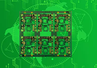
ceramic pcb board
Related technologies in ceramic pcb board substrate manufacturing processes:
1. Drilling: Mechanical drilling is used to create conductive pathways between metal layers.
2. Plating through-holes: After drilling the holes for copper interconnections between layers, the circuits between layers are not yet conductive. Therefore, a conductive layer must be formed on the hole walls to connect the circuits. This process is generally referred to as the ‘PTH process’ in the industry, and the main procedures include stripping, chemical copper plating, and electrolytic copper plating.
3. Dry film lamination: Creating a photosensitive resist layer for etching.
4. Inner layer circuit image transfer: Using exposure to transfer the image from the film onto the board surface.
5. Outer layer circuit exposure: After applying the photosensitive film, the circuit board undergoes a process similar to that of the inner layer board, including exposure and development. The primary function of the photosensitive film in this step is to define the areas that require electroplating and those that do not. The areas we cover are those that do not require electroplating
6. Magnetron sputtering: Utilising the energy and momentum exchange between positive ions generated during gas glow discharge and surface atoms of the target material, material is transferred from the source material to the substrate to achieve thin film deposition.
7. Etching — formation of external circuits: A technique that removes material through chemical reactions or physical impact. The functionality of etching lies in selectively removing material according to specific patterns.
After circuit line plating is completed, the circuit board is sent for film removal, etching, and tin line removal. The primary task is to completely remove the plating resist, exposing the copper to be etched to the etching solution. Since the top of the circuit area is protected by tin, an alkaline etching solution is used to etch the copper. However, since the circuits are protected by tin, the circuits in the circuit area are retained, resulting in the overall surface circuits of the circuit board being revealed.
8. Solder mask application: The purpose of ceramic circuit boards is to carry electronic components and achieve connectivity. Therefore, after the circuit board traces are completed, the areas for assembling electronic components must be defined, and the non-assembly areas must be appropriately protected with polymer materials. Since electronic components are assembled using solder, the polymer material used for local protection of the circuit board is called ‘solder mask.’ Currently, most photosensitive solder masks are applied using a wet ink coating process.
3. LAM Technology Process
1. High bonding strength between the metal layer and ceramic, excellent conductivity, capable of multiple welds, metal layer thickness adjustable between 1 μm and 1 mm, maximum L/S resolution of 10 μm, and convenient direct via connection.

ceramic pcb board
2. Advantages of LAM Technology:
(1) Higher thermal conductivity: The thermal conductivity of traditional aluminium-based circuit boards (MCPCB) is 1–2 W/m·K. Copper has a thermal conductivity of 383.8 W/m·K, but the thermal conductivity of the insulating layer is only around 1.0 W/m·K, with better ones reaching 1.8 W/m·K. The thermal conductivity of aluminium oxide ceramics is 20–35 W/m·K, and that of aluminium nitride ceramics is 170–230 W/m·K. The thermal conductivity of the copper substrate is 2 W/(m·K). Additionally, its thermal expansion coefficient matches that of commonly used LED chips, allowing large silicon-based chips to be directly mounted on the copper conductor circuit, eliminating the need for transition layers such as molybdenum sheets in traditional modules;
(2) Stronger and lower-resistance metal film layers: The bonding strength between the metal layer and the ceramic substrate is high, reaching up to 45 MPa (greater than the strength of the ceramic substrate itself at over 1 mm thickness); the metal layer has excellent conductivity, for example, the volume resistivity of copper is less than 2.5 × 10^(−6) Ω·cm, resulting in minimal heat generation when current flows;
(3) Good weldability and high operating temperature: resistant to welding and capable of repeated welding;
(4) Excellent insulation: withstand breakdown voltage up to 20 kV/mm;
(5) Conductive layer thickness customisable within 1 μm to 1 mm: current can be designed according to circuit module requirements; thicker copper layers allow higher current flow. Traditional DBC technology can only produce conductive layers with thicknesses between 100 μm and 600 μm; when producing layers thinner than 100 μm, the production temperature is too high and the material melts; when producing layers thicker than 600 μm, the copper layer is too thick, causing the copper to flow down and resulting in blurred edges on the product. Our copper foil is applied as a coating, allowing for customisation of thickness between 1 μm and 1 mm with high precision.
(6) Low high-frequency loss, enabling high-frequency circuit design and assembly; low dielectric constant;
(7) Supports high-density assembly, with line/spacing (L/S) resolution as low as 20 μm, enabling the miniaturisation, lightweight, and thin design of devices;
(8) Free of organic components, resistant to cosmic rays, high reliability in aerospace applications, and long service life;
These are the introduction to the manufacturing process of ceramic PCB Boards.