A Trustworthy PCB and Electronic Manufacturing Enterprise! Contact Us


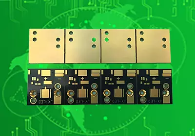

Product:Copper PCB (for low-to-medium current electronics).
Material: FR-4 substrate (Tg 130℃–150℃, cost-effective).
Quality Standard: IPC-2221, RoHS compliant.
Dielectric Constant: 4.2–4.7 @1MHz (suits<1GHz low-frequency use).
Layers: 1–8 layers (typically 2–4 layers).
Thickness: Substrate 0.4–1.6mm; overall board 0.6–2.0mm.
Copper Thickness: 0.5oz–3oz (18μm–105μm; 0.5oz for ultra-low power, 2–3oz for 5A–15A).
Surface Tech: OSP, lead-free HASL, or limited ENIG.
Operating Temp: -20℃ to +85℃.
Max Current: ≤15A (e.g., 2oz copper + 3mm width).
Applications: Consumer electronics, IoT sensors, prototyping, low-power industrial devices.
Copper PCB
In a world filled with consumer gadgets, household appliances, and simple industrial sensors, Copper PCB emerges as the reliable, accessible foundation for electronics that don’t demand extreme power or heat management. Unlike specialized high-power solutions, it prioritizes broad compatibility, cost-efficiency, and ease of integration for low-to-medium current applications—making complex electronics design feasible across diverse industries.
Core Advantages: Balancing Accessibility and Functionality
Flexible Copper for Diverse Needs:
Copper foils range from 0.5oz (18μm) (ideal for tiny sensors or USB chargers) to 3oz (105μm) (suited for small motor controls or IoT hubs). A 2oz copper layer with 3mm width safely carries 10A—enough for most consumer and low-power industrial use cases, without over-engineering for unnecessary power capacity.
Cost-Effective Manufacturing & Materials:
Built on standard FR-4 substrate (Tg 130℃–150℃), Copper PCB avoids the premium costs of high-power materials (like ultra-thick copper or ceramic). Mature processes (semi-additive etching, panel plating) enable 48-hour prototype turnaround and low mass-production costs—perfect for mass-market gadgets (e.g., wireless earbuds) or DIY projects.
Reliable for Routine Use Cases:
While not designed for extreme conditions, it excels in everyday reliability:
Surface Finishes: Choose OSP (eco-friendly for consumer devices), lead-free HASL (robust for prototyping), or ENIG (for 3–5 year product lifecycles).
Temperature Range: Operates stably from -20℃ to +85℃—sufficient for indoor/outdoor devices like smart thermostats or security cameras.
Standards Compliance: Meets IPC-2221 (general PCB design) and RoHS, ensuring basic quality and environmental safety.
Ideal for Mainstream Applications
Consumer Technology:
Powers smartphones (1oz copper for 5V/2A charging), laptops (2oz copper for USB-C ports), and home appliances (0.5oz copper for LED light controls).
IoT & Low-Power Industrial:
Enables sensor nodes (e.g., temperature/humidity sensors with 1oz copper for 3.3V signaling) and small control panels (e.g., office printer boards with 2oz copper for motor drivers).
Prototyping & Education:
Hobbyists and students use it for Arduino shields (1oz copper for 5V power) or custom LED projects (2oz copper for 12V strips).
Simple Customization for Any Project
Whether you’re building a consumer device, IoT prototype, or small appliance, our Copper PCB offers:
Layer Options: 1–8 layers (2-layer for simplicity, 4-layer for basic signal/power separation).
Size Flexibility: From 10mm×10mm (tiny sensors) to 300mm×300mm (large appliance control boards).
Fast Turnaround: 48-hour prototypes and 7–10 day mass production for time-sensitive projects.
For electronics that don’t need extreme power or heat management, Copper PCB delivers simplicity and value. Reach out to the IPCB technical team to explore how our standard Copper PCB can streamline your consumer, IoT, or low-power project.
Product:Copper PCB (for low-to-medium current electronics).
Material: FR-4 substrate (Tg 130℃–150℃, cost-effective).
Quality Standard: IPC-2221, RoHS compliant.
Dielectric Constant: 4.2–4.7 @1MHz (suits<1GHz low-frequency use).
Layers: 1–8 layers (typically 2–4 layers).
Thickness: Substrate 0.4–1.6mm; overall board 0.6–2.0mm.
Copper Thickness: 0.5oz–3oz (18μm–105μm; 0.5oz for ultra-low power, 2–3oz for 5A–15A).
Surface Tech: OSP, lead-free HASL, or limited ENIG.
Operating Temp: -20℃ to +85℃.
Max Current: ≤15A (e.g., 2oz copper + 3mm width).
Applications: Consumer electronics, IoT sensors, prototyping, low-power industrial devices.
iPCB Circuit provides support for PCB design, PCB technology, and PCBA assembly. You can request technical consultation or quotation for PCB and PCBA here, please contact email: sales@ipcb.com
We will respond very quickly.
