A Trustworthy PCB and Electronic Manufacturing Enterprise! Contact Us


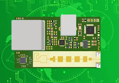
Wireless connectivity has become an invisible yet essential pillar of modern technology. From smart home sensors and cellular base stations to satellite communication links and automotive radar systems, millions of devices rely on high-frequency electromagnetic waves to transmit data across the air. Unlike low-frequency or direct-current circuits where electricity simply follows copper paths like water through a pipe, high-frequency signals behave like high-speed radio waves governed by complex electromagnetic physics. When operating in gigahertz frequency spectrums, minor layout flaws or trace geometry mistakes can cause severe signal reflections, power losses, and complete wireless communication failure. Mastering the principles of RF PCB design is the ultimate key for hardware engineers seeking to build reliable, high-performance wireless products that clear regulatory testing on the first try.
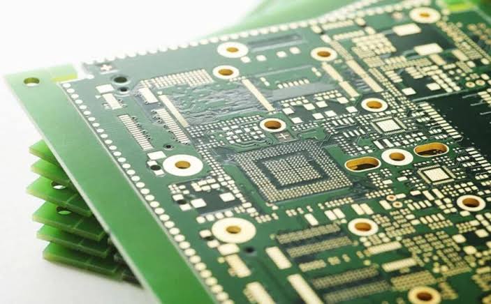
RF PCB Design
Selecting High Frequency Substrates and Low Loss Materials
The physical foundation of any radio frequency system starts with the choice of substrate material. In standard digital or low-speed audio electronics, inexpensive FR4 glass-epoxy composite boards serve as a reliable and economical base. However, standard FR4 exhibits a relatively high and unstable dielectric constant alongside a high dissipation factor at multi-gigahertz frequencies, causing it to absorb high-frequency energy and convert it into unwanted heat.
To prevent severe signal attenuation, high-frequency engineers utilize specialized fluoropolymer-based laminates or ceramic-filled hydrocarbon thermoset materials, widely known as Rogers or Taconic substrates. These advanced materials maintain a remarkably stable dielectric constant across wide temperature variations and provide an ultra-low loss tangent. By minimizing dielectric absorption, these high-end laminates ensure that delicate microwave signals travel smoothly from active transceiver chips out to the antenna without suffering from phase distortion or power degradation.
Mastering 50 Ohm Characteristic Impedance Matching
One of the most fundamental rules in any successful RF PCB design project is maintaining strict, continuous impedance matching throughout the entire transmission path, universally standardized at 50Ω for modern RF systems.
When high-frequency signals travel along copper traces, any sudden mismatch in trace width, substrate thickness, or ground reference distance creates a physical barrier that reflects energy backward toward the transmitter. These standing waves waste power and distort data packets. To prevent this, layout engineers calculate precise microstrip or stripline geometry—adjusting copper thickness, trace width, and dielectric height—to lock the characteristic impedance precisely at 50Ω. Furthermore, layout guidelines dictate that high-frequency traces must never feature sharp 90-degree corners. Sharp bends create localized capacitance concentrations that alter local impedance; instead, designers utilize smooth, curved radius routes or mitered 45-degree bends to keep signal flow undisturbed.
Grounding Strategies and Electromagnetic Interference Shielding
Controlling high-frequency return currents is another vital challenge encountered during advanced RF PCB design execution. At high frequencies, return currents do not simply take the path of least resistance back to the power source; instead, they flow directly underneath the signal trace on the nearest adjacent reference plane, hugging the trace geometry like a shadow.
A successful layout requires an unbroken, solid ground reference plane directly beneath every high-frequency signal layer. Interrupting this ground plane with split sections or routing low-speed digital lines across it forces return currents to take long, detoured routes, creating massive electromagnetic loops that radiate noise like an unwanted antenna. To lock down stray high-frequency energy, engineers implement dense rows of plated grounding vias—known as via stitching or via fencing—along the perimeter of sensitive RF traces. For extremely noise-sensitive transceivers, stamped metal shielding cans are soldered directly onto perimeter ground rings to box in electromagnetic radiation completely.
Component Placement and Power Supply Noise Suppression
Physical component arrangement directly dictates the electrical performance of a wireless circuit. In a professional RF PCB design workflow, component placement always takes precedence over simple aesthetic neatness. Active RF components, including power amplifiers, low-noise amplifiers (LNAs), mixers, and voltage-controlled oscillators, must be positioned as closely together as possible to keep interconnecting trace lengths exceptionally short.
Long traces act as parasitic inductors that degrade gain and alter frequency tuning. Additionally, power supply lines feeding these active components must be heavily filtered. High-frequency digital noise originating from microprocessors or switching regulators can easily leak through power pins into the RF chain, corrupting clean radio signals. Engineers combat this by placing multi-stage decoupling capacitor networks—featuring values ranging from microfarads down to picofarads—directly adjacent to every power pin, shunting high-frequency noise safely to ground before it can disrupt radio performance.
Conclusion
Developing high-frequency wireless electronics demands a complete shift in mindset compared to traditional low-speed digital hardware engineering. Treating radio frequency traces like ordinary copper wires inevitably leads to poor wireless range, failed compliance testing, and costly PCB respins. By utilizing low-loss microwave substrates, enforcing strict 50Ω impedance matching, maintaining solid ground reference planes, and optimizing component placement, your development team can overcome the toughest electromagnetic challenges. Investing the necessary engineering hours into precise RF PCB design guarantees that your wireless products deliver maximum transmission range, exceptional signal clarity, and absolute operational reliability in the competitive global tech market.