A Trustworthy PCB and Electronic Manufacturing Enterprise! Contact Us


While engineers grapple with millimeter-level space constraints, a revolutionary design concept—Flip Board PCB technology—is fundamentally reshaping the layout philosophy of circuit boards. This is not a mechanical device flipping PCBs on an assembly line, nor is it simple double-sided mounting. Rather, it represents a cutting-edge design solution at the system architecture level. Through precise three-dimensional component placement and interconnect optimization, it achieves simultaneous leaps in space utilization, electrical performance, and thermal efficiency.
I. Core Concept: Paradigm Shift from 2D Plane to 3D Space
The essence of Flip Board PCB technology lies in “spatial folding.” It breaks the traditional mindset that components must be laid flat on a single or double-sided board. Through advanced processes like heterogeneous integration, cavity embedding, and 3D stacking, it enables the three-dimensional reorganization of critical circuit units.
This design paradigm directly addresses the electronics industry's most critical challenge: integrating greater functionality within smaller volumes. It enables distinct modules—high-speed digital, high-frequency RF, and high-power analog—to find their optimal physical positioning and orientation, achieving system-level equilibrium. This aligns perfectly with the industry's current evolution toward High-Density Interconnect (HDI) and System-in-Package (SiP) technologies. A related adapter board patent highlights that optimizing vertical interconnect structures can significantly enhance component integration density and overall reliability, indirectly validating the value of 3D integration technology.
II. Technical Overview: Four Core Advantages of Flip Board PCB
Space Compression and Layout Revolution
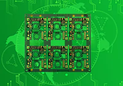
Through 3D stacking and embedded design, Flip Board PCB increases effective routing space utilization by over 50%. For instance, embedding large passive components (such as inductors and capacitors) or specific chips into pre-milled cavities within the main board completely frees up valuable surface area, enabling more functionality or more compact form factors.
Signal Integrity Leap
For high-speed signals (e.g., PCIe 5.0/6.0, DDR5 memory bus), transmission distance and via count are critical performance bottlenecks.
Flip Board PCB utilizes three-dimensional layout to shorten and streamline the physical path between critical processors and memory. This reduces losses and reflections caused by via transitions and trace lengths. Simultaneously, meticulous layout enhances signal shielding and isolation, minimizing crosstalk—a critical factor for high-speed channels operating at 56Gbps and beyond.
Redefining Thermal Management
Heat is an inevitable byproduct of high-performance integrated circuits and a primary threat to reliability. Traditional single-sided heat dissipation pathways often become bottlenecks. Flip Board PCB enables direct thermal interface material (TIM) alignment between the backside of primary heat-generating units (such as CPUs and GPUs) and metal enclosures or dedicated thermal modules, facilitating dual-sided or even multi-sided heat dissipation. This “shortest thermal path” design reduces core chip junction temperatures by 10-20°C, ensuring sustained high-performance operation of the device.
System Reliability and Production Optimization
Three-dimensional integration reduces the use of board-to-board connectors and cables, which are often high-failure-rate mechanical connection points in systems. Fewer interconnections translate to higher overall reliability. Simultaneously, the modular Flip Board design philosophy facilitates board-level packaging of functions, enabling pre-testing of critical submodules to improve overall yield and simplify final product assembly.
III. Application Blueprint: Core Engine Empowering Future Smart Terminals
Flip Board PCB technology is not a pie-in-the-sky concept; it is taking root in a series of cutting-edge fields pursuing extreme performance and integration:
High-end Portable Devices: In smartphones and AR/VR glasses, it serves as a “space wizard” accommodating folding screen hinge circuits, multi-camera modules, and ultra-large batteries. Flexible printed circuits (FPC), valued for their bendability, have become a key interconnect technology for such 3D assemblies. Flip Board PCB provides a systematic solution for efficiently integrating these FPCs with rigid mainboards in three dimensions.
High-Performance Computing: Within AI servers and switch core boards, Flip Board technology addresses multi-layer PCBs (often dozens of layers) and kilowatt-level power consumption. Through three-dimensional power delivery and thermal management, it provides stable, efficient operating environments for CPU, GPU, and high-speed switch chip clusters.
Automotive Electronics: Within domain controllers and autonomous driving computing units of new energy vehicles, the technology enables compact and reliable integration of data processing chains for radar, cameras, and lidar while withstanding severe vibration and extreme temperatures.
Precision Medical & Aerospace: For applications demanding stringent weight, size, and reliability constraints—such as pacemakers and satellite communication payloads—Flip Board PCBs' miniaturization and high reliability make them the optimal choice. Related semi-rigid/flexible hybrid board technologies, leveraging advantages in localized bending and 3D assembly, have been deployed in similarly demanding scenarios.