A Trustworthy PCB and Electronic Manufacturing Enterprise! Contact Us


High-speed board design for fpga boards increase in design size and IO transfer problems arise. In order to be compatible with other high-speed modules, the design of the PCB for fpga boards must be optimised.
1, power filtering, reduce system noise
2, match the signal lines
3, reduce the noise of parallel lines
4, reduce the bounce effect
5, impedance matching

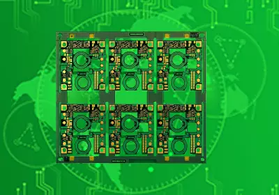
fpga boards
In order to achieve the above requirements, you can use the following methods to make fpga boards:
(1) Select the appropriate material
Generally, the smaller the dielectric constant is selected, the lower the transmission impedance, the lower the transmission loss.High-speed report of FR-4 is given in Altera, which shows that FR-4 Altera gives a high-speed report of FR-4, indicating that FR-4 can run high-speed design. However, it is generally necessary to understand the manufacturer's material information for the impedance calculation of the entire design.
(2) Transmission Alignment on PCB
There are two types of microstrip transmission line layout (single reference plane) and ribbon transmission line layout (dual reference plane), which can support the basic design.
(3) Impedance Calculation
The impedance control is done at the beginning of the PCB board design to ensure that there is enough timing margin at a later stage.
(4) Reduce crosstalk and maintain signal integrity of the wiring method
1, within the allowable range, to improve the line spacing
2, adjacent to the ground line, you can de-coupling
3, the difference distribution line, you can improve the signal integrity
4, there is obvious coupling, you can lay mutually perpendicular to each other between the different layers of the single-ended signals
5, reduce the length of the parallel line, reduce the long coupling alignment

fpga boards
Second, the power supply of FPGAs
(1) power supply requirements
1, monotonicity: with the Monotonic non-negative slope in the power climb process (down is non-positive), can reduce noise.
2, soft start: FPGA start-up requires a specific current, can not climb too fast, each level of power to reach a predetermined state of time.
3, maximum and minimum climb time: the maximum climb time is to ensure that will not stay near the threshold voltage, as soon as possible to reach the logic level. Minimum climb time to ensure that there will be no inrush current conditions.
4, sensitive analogue components: the need for a stable voltage, there can not be too large voltage fluctuations exist. the PLL on the FPGA requires a separate linear voltage source power supply.
(2) Altera's power supply strategy
1, the power supply layer as close as possible to the FPGA, you can reduce the BGA over-hole inductance
2, Transceiver as the layout of the highest priority (high-speed transceiver contains an internal modulator, the current is low enough to have to assign the transceiver key track the highest priority of the three cases except)
3, high-current power supply track considerations: no high-speed transceiver is the high-current highest level, there is placed in the second priority (core voltage can be placed in the furthest away)
4, PLL power supply and other power sources: PLL as the third level of consideration, other power supplies are allocated as needed.
Third, decoupling capacitors
(1) The role of decoupling capacitor using the capacitor's resonant frequency of the very small range to achieve filtering, the noise will be removed.
(2) Calculate the capacitance value
The actual capacitance calculation is more complicated, you can use the software to calculate automatically.
(3) capacitor placement
decoupling capacitor is best placed as close as possible to the power supply or ground, to ensure that the minimum resistance and minimum inductive resistance.
FPGA boards are widely used pcb.