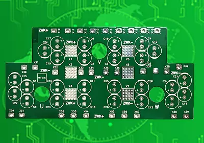
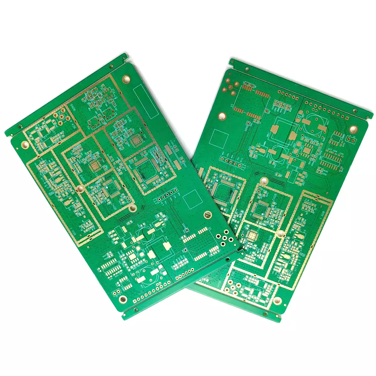
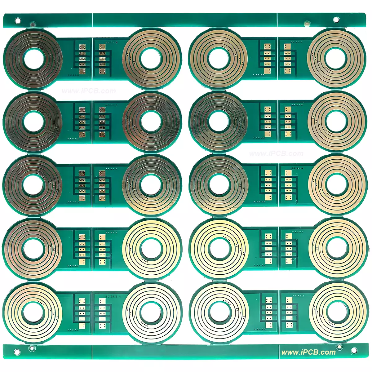
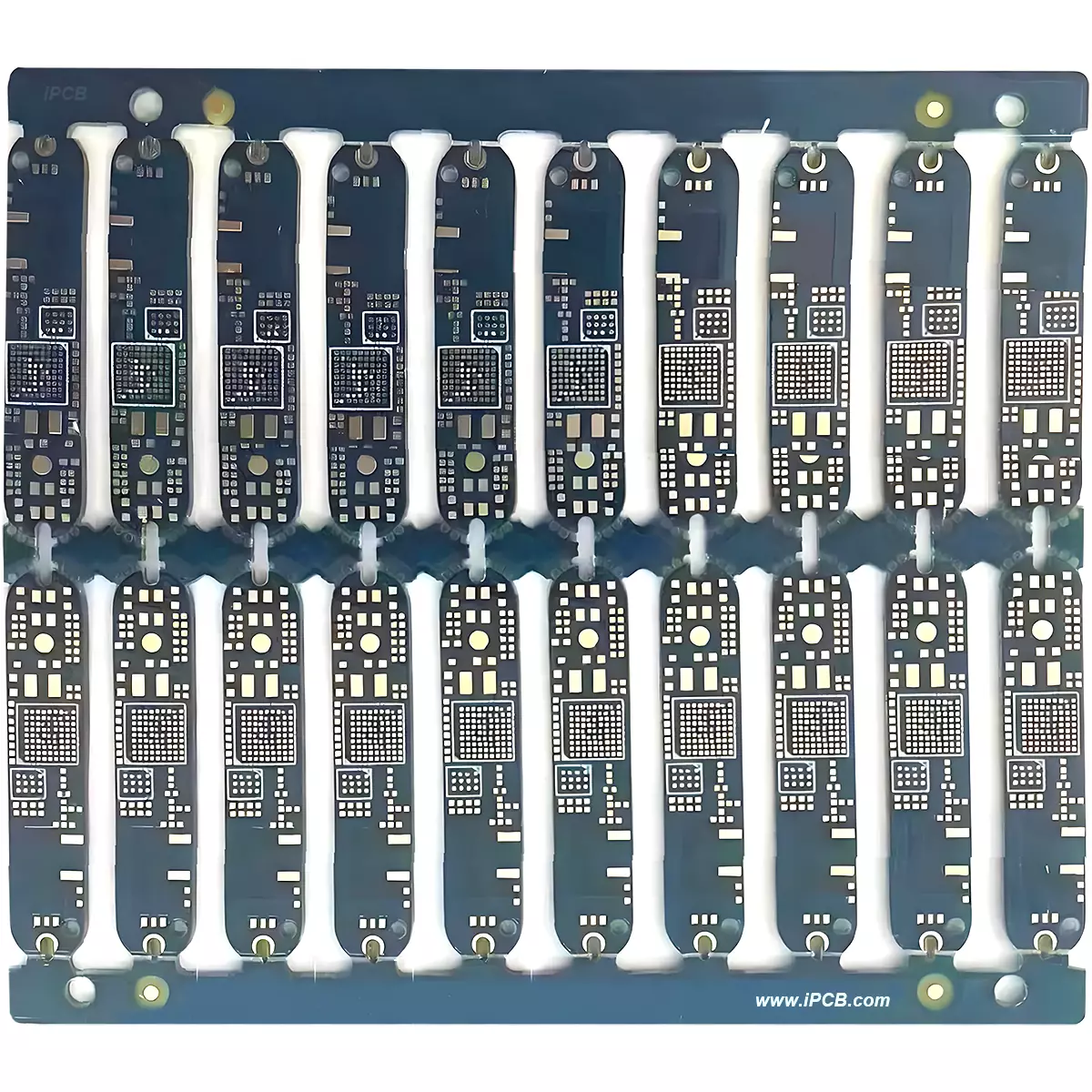
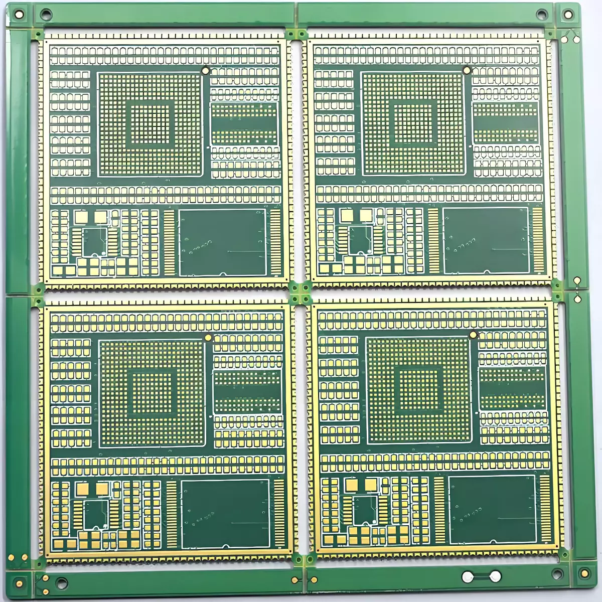
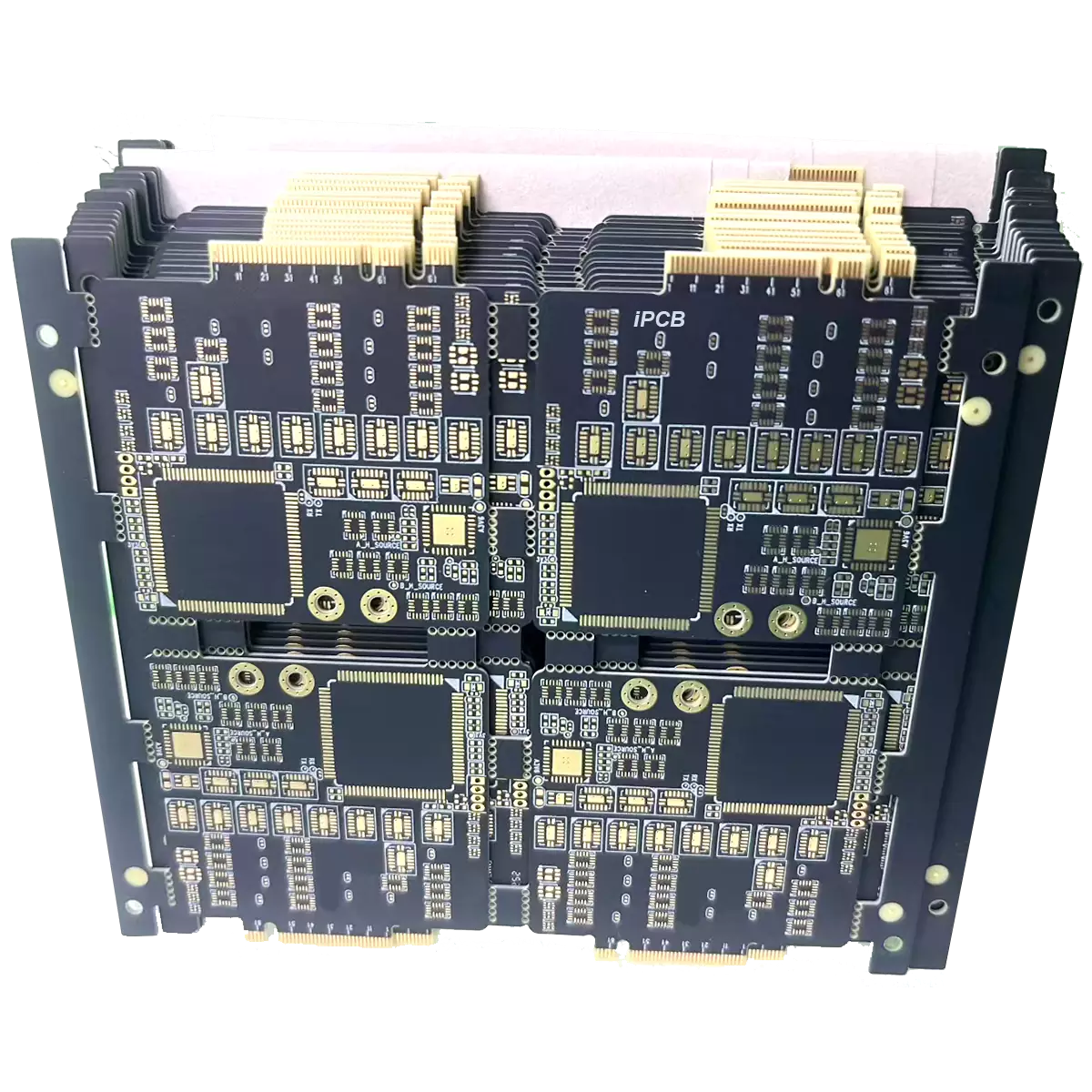
Product: FR-4 PCB Board (General-purpose flame-retardant PCB, the most widely used base material for low-to-medium frequency electronics)
Material: Glass fiber-reinforced epoxy resin composite; optional variants:
Common grade: Tg 130°C–150°C, suitable for general electronics.
High-Tg grade: Tg ≥170°C, for high-temperature scenarios (e.g., lead-free soldering).
Halogen-free grade: No bromine/chlorine, compliant with eco-sensitive fields (medical, wearables).
Quality standard:
Safety: UL94 V-0 (flame retardancy, per UL 94 standard).
Industry specs: IPC-6012 (PCB performance), IPC-TM-650 (test methods).
Environmental: RoHS 2.0 (2011/65/EU), REACH compliant.
Dk: 4.2–4.8 @1MHz–1GHz (per IPC-TM-650 2.5.5.13)
Layers: 1–12 layers
Thickness:
Substrate thickness: 0.4mm–3.2mm (customizable up to 8mm for thick-board needs).
Finished board thickness tolerance: ±0.1mm (for thickness ≥0.8mm, per IPC-6012).
Copper thickness: 0.5oz/ft² (18μm)–6oz/ft² (210μm); inner layers typically 0.5oz–1oz, outer layers optional thick plating (2oz–6oz) for high-current segments.
Surface technology:
HASL-LF (Lead-Free Hot Air Solder Leveling): Cost-effective, general-purpose.
ENIG (Electroless Nickel Immersion Gold): Flat surface, suitable for fine-pitch components (QFN/BGA) and gold fingers.
OSP (Organic Solderability Preservative): Eco-friendly, for single-reflow processes (short shelf life).
Immersion Silver/Tin: Enhanced solderability, for niche conductivity needs.
Special requirements:
High-Tg grade required for lead-free soldering (peak temp ≥260°C) or long-term use in 85°C+ environments.
Impedance control (50Ω/100Ω) needs manufacturer’s specific Dk value for simulation (Dk varies by batch).
Halogen-free grade mandatory for medical devices or EU eco-labeled products.
Application:
Consumer electronics: Smartphones, TVs, home appliances (refrigerators/washing machines).
Industrial: Control boards, sensors, low-frequency motor drivers.
Automotive: Non-high-frequency segments (infotainment, lighting control).
Power modules: Low-to-medium power DC-DC converters, LED drivers.