A Trustworthy PCB and Electronic Manufacturing Enterprise! Contact Us


Product: Gold plated PCB
Material: FR-4 (Tg 130–170°C) or Rogers (for high-frequency); Nickel underlayer + gold plating (purity ≥99.9%)
Quality standard: IPC-6012, ASTM B488, RoHS 2.0
Dielectric constant: 4.2–4.7
Layers: 2–32 layers
Thickness: 1.6mm (standard); Custom: 0.8–3.2mm (tolerance ±0.1mm)
Copper thickness: Inner: 0.5oz (≈17.5μm); Outer: 1oz (≈35μm) (up to 3oz for high-current needs)
Surface technology: ENIG (Electroless Nickel Immersion Gold, gold: 0.05–0.1μm; nickel: 3–6μm) or electroplated hard gold (0.5–2μm, for wear resistance)
Special requirements: Impedance control (50Ω±10% / 100Ω±10% for high-speed signals); Minimum line width/spacing: 3–5mil; High-temperature resistance
Application: 5G telecom base stations, medical diagnostic equipment, aerospace modules, industrial PLCs & robotics
When electronic devices demand long-term stability, anti-corrosion performance, and low-loss signal transmission—whether in 5G base stations, medical diagnostic equipment, or aerospace modules—Gold plated PCB stands out as a core component, leveraging gold’s inherent inertness and high conductivity to eliminate connectivity risks in harsh or high-precision scenarios.
Core Advantages: Material & Craftsmanship That Deliver Reliability
Each Gold plated PCB is built to strict specifications to meet critical industry needs:
Base Material: Adopts FR-4 (Tg 130–170°C) for general-purpose use, with optional Rogers substrates for high-frequency applications; the base ensures thermal stability even in temperature-fluctuating environments (e.g., industrial workshops or aerospace cabins).
Gold Plating Craft: Features a dual-layer structure of nickel underlayer (3–6μm) + gold plating (99.9% purity)—choose ENIG (Electroless Nickel Immersion Gold, 0.05–0.1μm gold) for fine-pitch soldering (e.g., BGA chips) or electroplated hard gold (0.5–2μm gold) for high-wear scenarios (e.g., frequent-insertion connectors).
Structural Flexibility: Supports 2–32 layers (typical 6–12 layers for complex systems) with standard thickness of 1.6mm (customizable 0.8–3.2mm, tolerance ±0.1mm); inner copper thickness of 0.5oz (≈17.5μm) and outer copper thickness of 1oz (≈35μm) (upgradable to 3oz for high-current modules like industrial PLC power units).
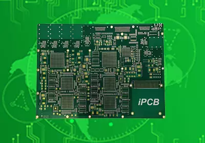
Gold plated PCB
Technical Performance: Meeting High-Precision Requirements
To ensure compatibility with high-speed, high-reliability systems, Gold plated PCB adheres to rigorous technical standards:
Dielectric Constant: 4.2–4.7 (@1MHz for FR-4 base), minimizing signal delay in data transmission;
Impedance Control: 50Ω±10% (single-ended) / 100Ω±10% (differential pair), ideal for 5G RF signals and medical imaging data transmission;
Fine Wiring: Minimum line width/spacing of 3–5mil, enabling integration of dense components (e.g., aerospace control chips).
Industry Applications: Trusted in Critical Sectors
Gold plated PCB is widely used in fields where failure is not an option:
5G Telecom: Powers 5G base station RF modules, with gold plating reducing signal insertion loss to ensure stable 10Gbps+ data throughput;
Medical Equipment: Used in ultrasound machines and diagnostic scanners, where anti-corrosion gold plating meets medical-grade hygiene and long-term reliability requirements;
Aerospace: Integrated into satellite communication modules, withstanding extreme temperatures (-55°C to +125°C) and vacuum environments;
Industrial Automation: Equips PLCs and robotic control units, resisting oil, dust, and humidity in factory settings to maintain 24/7 operation.
Quality Assurance & Customization
All Gold plated PCB products comply with IPC-6012, ASTM B488, and RoHS 2.0 standards, ensuring consistency and environmental friendliness. Whether you need high-frequency Rogers-based boards for 5G or hard gold-plated connectors for industrial robots, our team can tailor solutions to your specific layer count, thickness, and plating needs.
Ready to source reliable Gold plated PCB? Contact the iPCB technical team to submit your project requirements.
Product: Gold plated PCB
Material: FR-4 (Tg 130–170°C) or Rogers (for high-frequency); Nickel underlayer + gold plating (purity ≥99.9%)
Quality standard: IPC-6012, ASTM B488, RoHS 2.0
Dielectric constant: 4.2–4.7
Layers: 2–32 layers
Thickness: 1.6mm (standard); Custom: 0.8–3.2mm (tolerance ±0.1mm)
Copper thickness: Inner: 0.5oz (≈17.5μm); Outer: 1oz (≈35μm) (up to 3oz for high-current needs)
Surface technology: ENIG (Electroless Nickel Immersion Gold, gold: 0.05–0.1μm; nickel: 3–6μm) or electroplated hard gold (0.5–2μm, for wear resistance)
Special requirements: Impedance control (50Ω±10% / 100Ω±10% for high-speed signals); Minimum line width/spacing: 3–5mil; High-temperature resistance
Application: 5G telecom base stations, medical diagnostic equipment, aerospace modules, industrial PLCs & robotics
iPCB Circuit provides support for PCB design, PCB technology, and PCBA assembly. You can request technical consultation or quotation for PCB and PCBA here, please contact email: sales@ipcb.com
We will respond very quickly.
