A Trustworthy PCB and Electronic Manufacturing Enterprise! Contact Us


Product: Golden Finger PCB
Material: FR-4 (Grade A, Tg 130-170°C); Optional TU-872 SLK (high-frequency) or aluminum substrate (thermal management); Epoxy solder mask
Quality standard: IPC-6012, IPC-A-610
Dielectric constant: 4.2-4.7
Layers: 1-32 layers (common: 6-8 layers for industrial use)
Thickness: 0.2-4.5mm (standard 1.6mm); Tolerance ±0.1mm (≥0.8mm)
Copper thickness: Inner: 0.5oz (17.5μm); Outer: 1-2oz (35-70μm); High-power up to 3oz
Surface technology: Selective gold plating on fingers (0.25-1.3μm); ENIG for other areas; Optional HASL/OSP
Special requirements: Finger chamfer angle 20°-90° (typical 45°); Finger pitch ≥0.15mm; Impedance control 50Ω ±10% (RF paths); ≥1mm distance from fingers to board edge
Application: Computers (RAM, graphics cards), industrial PLCs, telecom routers, aerospace avionics, consumer electronics (USB connectors)

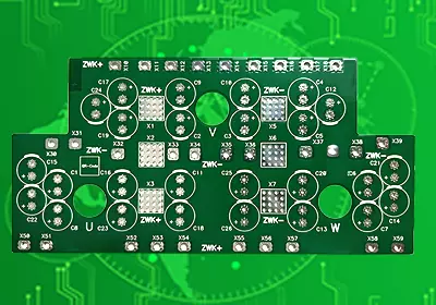
Golden Finger PCB
When reliable, high-performance board-to-board connections are non-negotiable, the Golden Finger PCB stands out as a core solution. Featuring gold-plated edge contacts (0.25–1.3μm thickness), it leverages gold’s low resistance and corrosion resistance to enable stable signal and power transmission—even through frequent insertions (1,000+ cycles) and harsh environments. Built with FR-4 (Tg 130–170°C, optional TU-872 SLK for high-frequency scenarios) and 1–32 layers, it balances durability with flexibility to meet diverse application needs.
This PCB powers critical applications across industries: Computers rely on it for DDR5 memory modules (supporting 5600MT/s high-speed reading and writing); industrial PLCs use it to connect control modules in semiconductor manufacturing equipment; 5G base stations adopt it for low-loss signal transmission between processing boards; medical MRI devices depend on it for stable connections between power and signal modules; smart watches use it to link motherboards with sensors in slim, compact designs. Each use case taps into its 50Ω ±10% impedance control (for RF paths) and 45° chamfered fingers (for easy, accurate insertion).
Backed by IPC-6012, RoHS 2.0, and optional AEC-Q200 certification, it’s fully customizable in terms of layer count, copper thickness (0.5–3oz), and surface finish (selective gold plating + ENIG). Whether you’re designing computing hardware, industrial automation tools, or consumer electronics, it delivers consistent, long-lasting connectivity.
Product: Golden Finger PCB
Material: FR-4 (Grade A, Tg 130-170°C); Optional TU-872 SLK (high-frequency) or aluminum substrate (thermal management); Epoxy solder mask
Quality standard: IPC-6012, IPC-A-610
Dielectric constant: 4.2-4.7
Layers: 1-32 layers (common: 6-8 layers for industrial use)
Thickness: 0.2-4.5mm (standard 1.6mm); Tolerance ±0.1mm (≥0.8mm)
Copper thickness: Inner: 0.5oz (17.5μm); Outer: 1-2oz (35-70μm); High-power up to 3oz
Surface technology: Selective gold plating on fingers (0.25-1.3μm); ENIG for other areas; Optional HASL/OSP
Special requirements: Finger chamfer angle 20°-90° (typical 45°); Finger pitch ≥0.15mm; Impedance control 50Ω ±10% (RF paths); ≥1mm distance from fingers to board edge
Application: Computers (RAM, graphics cards), industrial PLCs, telecom routers, aerospace avionics, consumer electronics (USB connectors)
iPCB Circuit provides support for PCB design, PCB technology, and PCBA assembly. You can request technical consultation or quotation for PCB and PCBA here, please contact email: sales@ipcb.com
We will respond very quickly.