A Trustworthy PCB and Electronic Manufacturing Enterprise! Contact Us


Product: Half Hole PCB
Material: FR-4 (Grade A, Tg 130-160°C); Optional aluminum substrate for thermal management; Epoxy UV-curable solder mask (10-15μm)
Quality standard: IPC-6012, IPC-A-610
Half-hole specs:
Diameter: 0.3-1.0mm (standard 0.6mm, min 0.5mm with process control)
Spacing: ≥0.35mm (recommended ≥0.45mm)
Hole wall copper: ≥25μm (electroless copper plating + electrolytic plating)
Position accuracy: ±0.05mm (edge-aligned)
Layers: 1-24 layers (common: 2-8 layers for modular designs)
Thickness: 0.6-3.2mm (standard 1.6mm); Tolerance ±0.1mm (≥0.8mm)
Copper thickness: 0.5-3oz (17.5-105μm); High-power up to 5oz
Surface finish: ENIG (4-6μm Ni, 0.05-0.1μm Au); Optional HASL, OSP, immersion silver
Special requirements:
Half-hole to edge distance: ≥1mm
Solder mask opening over closed half-hole areas
Impedance control: 50Ω ±10% (for RF paths when needed)
Application: Modular electronics (motherboard-daughterboard links), LED modules, automotive sensors, smart wearables
When compactness, reliability, and seamless board-to-board integration are critical, the Half Hole PCB transforms how electronics are built. These specialized circuit boards use precision-plated half-holes to replace bulky connectors, slashing assembly complexity while maximizing space efficiency—perfect for designs where modules must link tightly without compromising performance. Whether you’re engineering stacked IoT systems, LED arrays, or automotive sensor networks, this PCB redefines modular design.
Engineered for Precision Modularity
The Half Hole PCB is purpose-built to simplify interconnected, space-constrained projects:
Integrated “Connectors”: Plated half-holes (0.3–1.0mm diameter, with ≥25μm copper plating) act as built-in board-to-board links. This lets PCBs stack vertically or join edge-to-edge without extra hardware—cutting assembly time, shrinking product size, and boosting reliability (no loose connectors to fail).
Robust, Adaptable Build: Constructed with FR-4 (Tg 130–160°C) for thermal stability, plus ENIG surface finish (4–6μm Ni, 0.05–0.1μm Au) for corrosion resistance and flawless soldering. Available in 2–8 layers to fit dense circuitry into tight spaces, with optional aluminum substrates for heat dissipation in power-hungry modules.
Fully Customizable: Tailor thickness (0.6–3.2mm), copper weight (0.5–5oz), and impedance (50Ω ±10% for RF paths) to match low-power wearables, high-current automotive systems, or wireless IoT devices.
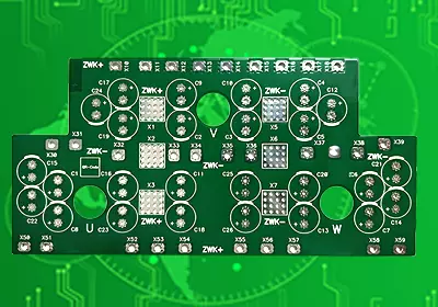
Half hole PCB
Powering Innovation Across Industries
Half Hole PCBs are the backbone of modular design in key sectors:
IoT & Smart Devices:
Home & Commercial IoT: Stackable mother-daughterboard setups for smart routers (where half-holes link WiFi, Bluetooth, and power modules into a single compact unit).
Industrial Sensors: Modular factory IoT nodes where half-holes connect sensing, processing, and communication boards to survive vibration and tight enclosures.
LED & Lighting:
Architectural Lighting: Modular LED panel drivers where half-holes let multiple PCBs join into large, uniform arrays (e.g., museum display lighting with slim, seamless profiles).
Automotive Lighting: Headlight control modules where half-holes connect LED driver boards to thermal management substrates without bulk.
Automotive & Transportation:
ADAS Systems: Sensor modules (like 360° camera arrays) where half-holes link imaging PCBs to processing boards—resisting shock and vibration better than connectors.
Electric Vehicles: Battery management system (BMS) modules where half-holes connect cell-monitoring PCBs into a unified stack for efficient power distribution.
Wearable Technology:
Smartwatches & Hearables: Tiny stacked PCBs for displays, sensors, and wireless chips—linked via half-holes to fit complex tech into wrist or ear form factors.
Backed by IPC-6012 standards, RoHS 2.0 compliance, and optional AEC-Q200 certification for automotive use, the Half Hole PCB is ready to elevate your modular design.
Product: Half Hole PCB
Material: FR-4 (Grade A, Tg 130-160°C); Optional aluminum substrate for thermal management; Epoxy UV-curable solder mask (10-15μm)
Quality standard: IPC-6012, IPC-A-610
Half-hole specs:
Diameter: 0.3-1.0mm (standard 0.6mm, min 0.5mm with process control)
Spacing: ≥0.35mm (recommended ≥0.45mm)
Hole wall copper: ≥25μm (electroless copper plating + electrolytic plating)
Position accuracy: ±0.05mm (edge-aligned)
Layers: 1-24 layers (common: 2-8 layers for modular designs)
Thickness: 0.6-3.2mm (standard 1.6mm); Tolerance ±0.1mm (≥0.8mm)
Copper thickness: 0.5-3oz (17.5-105μm); High-power up to 5oz
Surface finish: ENIG (4-6μm Ni, 0.05-0.1μm Au); Optional HASL, OSP, immersion silver
Special requirements:
Half-hole to edge distance: ≥1mm
Solder mask opening over closed half-hole areas
Impedance control: 50Ω ±10% (for RF paths when needed)
Application: Modular electronics (motherboard-daughterboard links), LED modules, automotive sensors, smart wearables
iPCB Circuit provides support for PCB design, PCB technology, and PCBA assembly. You can request technical consultation or quotation for PCB and PCBA here, please contact email: sales@ipcb.com
We will respond very quickly.
