A Trustworthy PCB and Electronic Manufacturing Enterprise! Contact Us


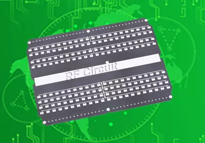
As wireless communication networks evolve toward higher frequency bands, traditional circuit board substrates face serious physical limits. Technologies like 5G infrastructure, millimeter-wave automotive radar, satellite communication links, and advanced aerospace telemetry systems require data transmission at multi-gigahertz speeds. Under these extreme high-frequency conditions, standard glass-epoxy materials like FR4 cause unacceptable signal attenuation, severe phase distortion, and excess heat accumulation. To maintain signal clarity across microwave and millimeter-wave frequencies, RF engineers rely on specialized fluoropolymer laminates. Utilizing a high-grade PTFE PCB material offers extraordinarily low dielectric constants and minimal signal loss, providing an ultra-stable foundation for demanding high-frequency electronic designs.
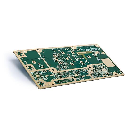
PTFE PCB material
Key Electrical and Thermal Properties
The outstanding microwave performance of PTFE (polytetrafluoroethylene), commonly known as Teflon, stems directly from its unique molecular structure. The strong chemical bonds between carbon and fluorine atoms yield a non-polar polymer with remarkable electrical insulation capabilities.
---Low Dielectric Constant (Dk): PTFE laminates typically exhibit a very low Dk between 2.1 and 2.6. A lower Dk allows electrical signals to travel faster through copper traces, significantly reducing signal propagation delay across the circuit.
---Minimal Dissipation Factor (Df): With a Df value as low as 0.0008 to 0.0015 in the gigahertz spectrum, energy loss converted to heat is virtually negligible. This low loss ensures crisp signal integrity over long trace pathways.
---Thermal and Chemical Resistance: PTFE maintains stable electrical properties across a wide temperature window from -200℃ to +260℃. Furthermore, its near-zero moisture absorption rate prevents humidity from altering the substrate's dielectric performance out in the field.
Primary High Frequency Applications
Because of its unparalleled signal transmission efficiency, selecting a PTFE PCB material has become standard practice across critical telecom and aerospace sectors.
In modern telecommunications, 5G massive MIMO base station antenna arrays depend heavily on PTFE substrates to route radio signals without power loss. In automotive safety, 77 GHz collision-avoidance radar systems utilize ceramic-filled PTFE boards to process dense radar reflections with pinpoint spatial accuracy. Furthermore, satellite communication (SATCOM) ground terminals and military avionics platforms specify these fluoropolymer laminates for high-power RF power amplifiers and low-noise receivers, where signal clarity cannot be compromised.
Manufacturing and Processing Challenges
While PTFE provides unmatched electrical performance, its physical softness and non-stick chemical nature present unique fabrication challenges for circuit board manufacturing plants. Processing a PTFE PCB material requires specialized factory tooling and modified chemical treatment steps.
Because pure PTFE is naturally soft and prone to plastic deformation under pressure, drilling component through-holes requires ultra-sharp carbide drill bits spinning at high speeds to prevent burrs or smeared material inside the holes. Furthermore, the non-stick property that makes PTFE famous in cookware makes it notoriously difficult for electroplated copper to bond to hole walls. Fabrication facilities must perform specialized surface activation—typically using sodium-naphthenate chemical baths or high-power plasma etching—to prep the hole walls before applying chemical copper plating.
Comparing PTFE with Traditional Substrates and Rogers Materials
Understanding where fluoropolymer laminates fit into the broader substrate landscape helps design teams balance electrical performance against total manufacturing budget.
When compared to standard FR4, a PTFE PCB material offers vastly superior high-frequency signal retention, as FR4's higher Df causes severe signal absorption above 1GHz. However, pure PTFE suffers from a high Coefficient of Thermal Expansion (CTE), which can strain copper vias during thermal cycling. To solve this, advanced material suppliers reinforce pure PTFE resins with woven glass fibers or micro-ceramic fillers. These reinforced hybrid laminates (often produced by brands like Rogers, Taconic, or Isola) combine the electrical advantages of PTFE with improved mechanical stiffness and thermal stability, making them much easier to process in standard multilayer press lines.
Conclusion
Mastering thermal and electrical signal losses is vital for building next-generation high-frequency hardware platforms. Relying on standard FR4 for gigahertz-range designs leads to degraded wireless range, noisy data channels, and overheating active components. Choosing a certified PTFE PCB material gives hardware developers the low dielectric constant, minimal loss tangent, and environmental resistance required to conquer difficult microwave engineering tasks. By pairing precision impedance trace routing with an experienced PCB fabrication partner capable of handling plasma hole activation and high-speed drilling, your engineering team can deliver high-performing RF products that maintain flawless connection stability in the most challenging wireless environments worldwide.