A Trustworthy PCB and Electronic Manufacturing Enterprise! Contact Us

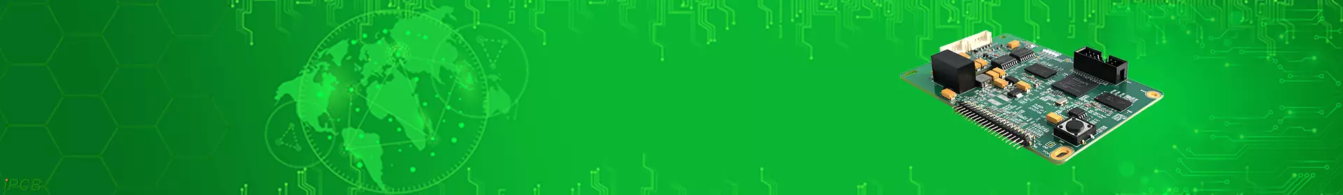
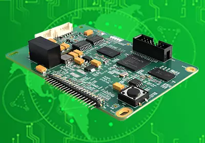
How to achieve main pcb assembly?Main pcb assembly–Main Printed Circuit Board Assembly.It is a printed circuit board on which all the electronic components are mounted.
1.What is PCB?
PCB – Printed circuit board. Technically, the term PCB refers to the etched circuit board itself with no components installed. Since printed circuit design often affects device functionality, the IPC Technical Executive Committee designated the term as a term for the development of new documents in 1999.Printed circuit boards or PCBs are at the heart of any electronic device. It has two main features:Accommodates electronic components, connects components for operation.The plate itself is made of a non-conductive substrate, such as fiberglass, which is coated with copper on one or both sides. Copper conducts electricity and is etched off the board, leaving the appropriate components to connect to each other by circuitry.

main pcb assembly
2.How does a printed circuit board work?
PCBA is designed to provide a central hub for integrating all the electronic components in a device. Using multiple layers to create plates, conductive paths or lines can be laminated onto a substrate material.These copper traces are used to conduct electricity as circuits that are soldered to all components on the board, thus powering the device while providing insulation and safe current transfer.
3.What is the PCB made of?
The board itself consists of four key components:Substrate – The basis of a PCB, the substrate is usually made of fiberglass or some other non-conductive material. The substrate can be single or multi-layered.Copper – Used to transmit electric current, copper in the PCB replaces the wires.
Solder mask – A metal used to create a connection between the surface of a PCB and an electronic component. The solder mask protects the electronic traces underneath from adverse conditions.Wire mesh - a layer used to mark the connecting lines of electronic components, warnings and other devices with specific characteristics.
Before moving on to the final PCB production, the prototype must be validated to ensure that all components are connected and working properly to power the device
4.What is PCB Assembly?
A PCB is a physical structure made of laminated material, typically FR-4, that is used to structurally support and connect electronic components through copper traces and conductive pathways. PCBs are made by laminating copper sheets into a dielectric substrate and mounting chips and other components. One common substrate material is an epoxy glass composite, known as FR4, which is an abbreviation for "flame retardant" where the number "4" is specified for braided glass reinforcement resin.
Component types can be broadly divided into passive components and active components. Passive components do not contribute to the amplification of the circuit. It does not require inputs, only signals to work, such as resistors, capacitors, inductors, transformers, etc. Active components, on the other hand, can amplify signals and control input voltages or currents. Active components include integrated circuits (ICs), MOSFETs, diodes, transistors, and more.
PCB assembly is the process of soldering electronic components onto a bare PCB. The fully functional circuit board is then ready for use in the electronics.

main pcb assembly
5.What are the different assembly methods in the PCB assembly process?
There are two assembly methods to add components to a printed circuit board: the through-hole process and the surface mount process. In the through-hole process, component leads are inserted into a through-hole on the other side of the PCB. If mechanical strength is the primary requirement, it is the preferred method for assembling connectors. The surface mount process is the more primary method of soldering components into PCB pads, especially for higher density and lower cost options.
6.What are the key processes in main PCB assembly?
Solder printing
Solder printing is a method of printing solder material through a stencil into a PCB using a metal scraper to create a consistent volume of solder paste. Several lead-free alloys are used as solder pastes, such as SAC, which is short for SnAgCu (tin, silver, copper). The melting point of this ingredient is around 217 to 220 degrees Celsius. The size of the solder material deposited on the PCB depends on the size of the template aperture. Defects that can be encountered during the solder printing process are solder bridging and too much solder.
Component placement
Pick and place or die mounters are used to mount components into a PCB and hold them in place with wet solder material. As component density increases and size decreases, placement accuracy becomes more and more important. SMT machines consist of component feeders, which can be either ribbon or tray. The placement arm may consist of multiple nozzles that are used to pick and place components into the PCB. During PCB assembly, proper and precise placement of components is essential to ensure good quality.
Reflow soldering process
After the components are placed, the PCB undergoes a reflow process that melts and solidifies the solder. The solder must be heated above the specified melting point for the alloy to collapse and bond to the interface. The quality of the solder joints is affected by the soaking time and temperature and can be monitored using the reflow curve. Extreme temperatures can damage the board, so an engineering evaluation should be performed to determine the optimal temperature and time based on solder characteristics and board thermal sensitivity.
After all steps,you will achieve main pcb assembly.