A Trustworthy PCB and Electronic Manufacturing Enterprise! Contact Us


The rapid evolution of electronics has intensified the demand for PCB reverse engineering (RE), particularly for legacy system maintenance, intellectual property analysis, and failure diagnostics. Among the critical phases of RE, PCB-to-Schematic conversion stands as the cornerstone, enabling engineers to decode the functional logic of a physical board into a human-readable schematic. This process bridges the gap between obsolete hardware and modern design practices, offering insights into circuit behavior, component interactions, and signal integrity

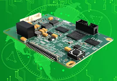
pcb to schematic
The concept of PCB Reverse Engineering
PCB to schematic reverse engineering is a step-by-step process of taking apart existing circuit boards, studying their parts, arrangement, and how they work, and turning the design files (schematics, PCB layout, bill of materials/BOM) around to match the original design. Its main goal is to understand the original design logic so that it can replicate, improve, or innovate hardware solutions. This is especially important when rebuilding old boards or analyzing competitive products where the original documents are missing.
Advantages of Reverse Engineering PCBs
PCB to Schematic Reverse Engineering enables the systematic recreation of circuit logic from physical PCBs, even when components or documentation are unavailable. By analyzing traces, components, and layer structures, this process extracts design intent to generate accurate schematics, PCB layouts, and BOMs. It empowers teams to repair, replicate, or modernize legacy boards while bypassing reliance on obsolete suppliers.
A core strength lies in its ability to decode PCB functionality into schematics without original files. High-resolution imaging and signal path tracing reconstruct power distribution, signal flows, and embedded protocols. This knowledge transfer reduces dependency on external experts—teams gain deep insights into EMI shielding, impedance control, and thermal management strategies, accelerating diagnostics and iterative upgrades.
The PCB to schematic workflow also drives competitive innovation. By reverse-engineering rival products, companies identify over-engineered circuits or material redundancies, enabling cost-optimized redesigns. Simultaneously, it reveals patent-compliant workarounds or performance-enhancing techniques. For obsolete systems, recovered schematics allow component substitution with modern equivalents, extending product lifecycles. Bridging physical hardware with abstract design logic, this process transforms legacy analysis into forward-looking R&D advantages, merging cost efficiency with strategic IP development.
PCB Reverse Engineering Process
1.Information collection
Record the model, parameters and location of all components on the PCB, shoot/scan and save the physical layout to ensure the traceability of subsequent analysis.
2.Layered analysis
Use high-resolution scanning or X-ray imaging technology to obtain images of each layer of the PCB, use software (such as Altium, KiCad) to identify the routing network, and distinguish the top layer, bottom layer and inner layer lines.
3.Functional module division
According to the component type (such as power chip, MCU, sensor) and routing characteristics (such as power wide line, signal thin line), the circuit is divided into functional units such as power management, signal processing, and communication interface.
4.Logic reconstruction
Use core components (such as processors, dedicated ICs) as reference points, combine data manuals to analyze pin functions, deduce peripheral circuit connection logic, and gradually build a complete schematic framework.
5.Verification and optimization
By cross-comparing the physical PCB with the generated schematic, test key node signals (such as voltage, waveform), correct connection errors and optimize drawing readability.

pcb to schematic
By following these steps, engineers can effectively reverse engineer a PCB schematic to gain a detailed understanding of the circuit design and functionality. This process is essential for solving problems, maintaining equipment, improving designs, and copying existing electronic designs.
Summary
The process of converting a PCB into a schematic (a diagram of the electrical connections) is important in the electronics field. It has many benefits, including making maintenance, innovation, and documentation easier. By converting the physical layout of a PCB back to a schematic, engineers can learn important things about the design and functionality of electronic circuits. Whether you're fixing an old system, improving an existing design, or studying a competitor's product, reverse engineering is a useful tool for improving technology and keeping electronic devices working well.