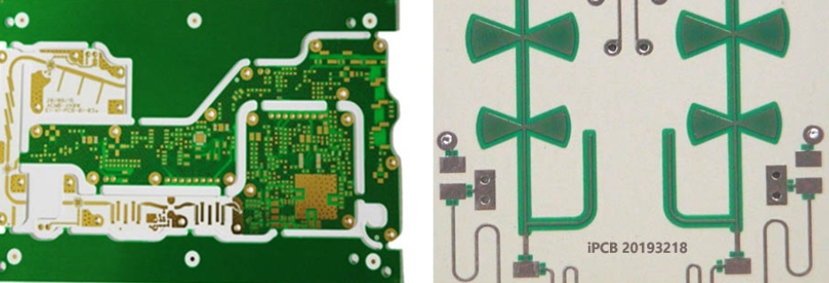
Microwave PCBs are printed circuit boards with RF or microwave signals above 50 MHz. Digital design applications require high circuit speeds, and the design of microwave PCBs have strict requirements for impedance control, proper grounding, and efficient signal routing to ensure the final product works efficiently.

microwave pcb design
Advantages of Microwave PCBs
-Higher speeds and faster data rates: Microwave PCB designs and applications are better at sending information quickly than lower-frequency circuit designs and applications.
-Less delay: It also has less propagation delay.
-Greater Bandwidth: As frequency goes up, the system can handle more channels, which increases its capacity.
-Higher resolution: Higher frequencies produce better resolution, which can be used for medical imaging and radar communications.
-Reduced size: Higher frequencies mean shorter wavelengths, which means that the antennas can be made smaller and more compact. This is an important factor for wearables and cell phones.
Challenges of Microwave PCBs
Microwave PCB design has its challenges, which are different from those for low-frequency circuit boards. Microwave frequencies (1 GHz to 30 GHz) cause problems like impedance mismatches, signal loss, crosstalk, and EMI because of short wavelengths and high signal velocities. So, it is very important to deal with parasitic components, manage skinning, and control transmission line behaviour when designing printed circuit boards for microwave frequencies. These factors make the design process more difficult, as small changes to the layout can harm performance.
1. Microstrip Line Impedance Mismatch
Microstrip line impedance mismatch occurs when the impedance of the line is different from the design value when a signal is sent through it. This can lead to signal loss, increased reflection, and other problems. Impedance matching is especially important in the high-frequency microwave field because it affects how stable the signal is and how well it can be transmitted.
2. Skin effect loss
When you design PCBs for microwaves, the higher the frequency, the more obvious the skin effect of the conductor becomes. At higher frequencies, the electrons mainly flow along the outer surface of the conductor. This is called the skin effect. It limits the current to a smaller area, so some of the signal energy is converted into heat. This is known as skin effect loss. To reduce this loss, it's important to make sure the PCB has the right impedance matching, and sometimes gold plating is needed.
3. Crosstalk
Crosstalk is when energy is accidentally transferred between conductors, which causes the signals to be coupled together. The problem of crosstalk is directly related to the edge rate of the active line. This makes it a big challenge for the design of microwave PCB boards. These problems are usually caused by mutual inductance and shunt capacitance, and crosstalk tends to increase as PCB density and performance increase. To reduce these coupling effects, we need to use special design methods. These include making sure that things are lined up properly, keeping the ground plane separate, and using controlled anode impedance.

microwave pcb design
8-Point Strategy to Address Microwave PCB Challenges
1. Make sure the widths of the wires are all the same so that there is no problem with the signals, and as much power as possible can be transferred by matching the characteristic impedance (50 ohms).
2. To avoid skin effect losses, make sure the thickness is set to 0.1 times the skin depth of the material. This will reduce the conversion of energy to heat.
3. It reduces crosstalk (signals getting mixed up) by putting protective wires between important signal lines, which solves one of the main problems in microwave PCB design.
4. To stop the circuit getting weaker and the signal getting worse, don't accidentally short out the RF alignments.
5. Avoid signal reflections by making sure that transmission lines are connected to loads that are the same as the characteristic impedance.
6. Make sure your signal traces are shorter than 1/20th of the wavelength. This will reduce signal loss and improve impedance control.
7. To stop interference, separate the power and ground layers in the inner PCB. This also reduces signal trace lengths to minimise crosstalk.
8. Make sure you have a ground plane to keep the ground voltage the same and stop problems with picking up EMI.
Microwave PCB design faces many challenges, largely due to the unique behavior of high-frequency signals. These challenges can be significantly mitigated by maintaining consistent impedance, utilizing proper trace lengths, controlling crosstalk through proper spacing and shielding, and employing advanced grounding techniques.