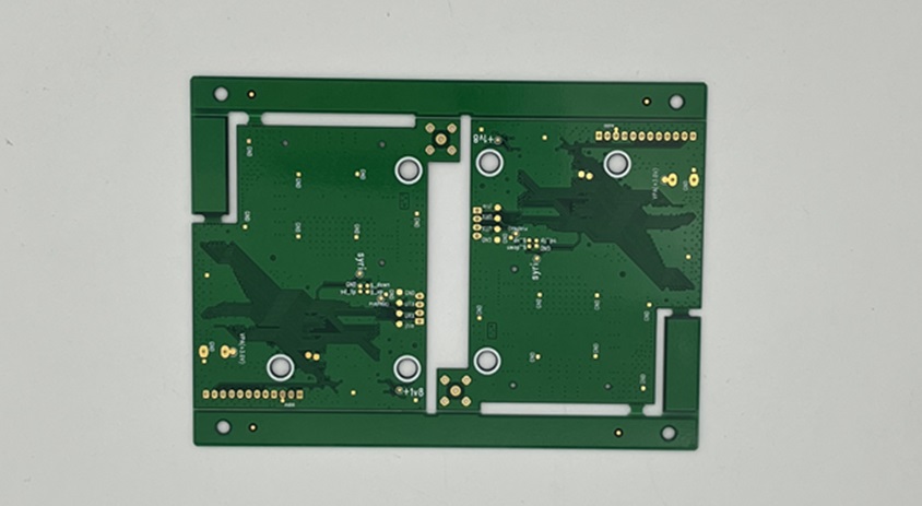
In the early days of electronics hobbyism, the "Toner Transfer" method—using a household iron to melt laser toner onto copper—was the gold standard. However, as components have shrunk from massive through-hole resistors to microscopic surface-mount devices (SMD), the old ways are no longer sufficient. If you are working with modern ICs like QFN or BGA, you need to learn how to print a PCB board using the UV Photoresist method. This technique bridges the gap between a "garage project" and a professional prototype, allowing for trace widths and clearances that were once only possible in industrial factories.

how to print a pcb board
Why is Toner Transfer Fading?
The fundamental problem with heat-based transfer is inconsistency. Heat expands the paper and squashes the toner, leading to "smashed" traces that cause short circuits. When your design requires 6-mil or 8-mil traces (the thickness of a human hair), even a 1% distortion is fatal.
This is where the UV (Ultraviolet) Photoresist method excels. Instead of mechanical pressure and heat, this process uses light and chemistry. By utilizing light-sensitive coatings, the resolution of your circuit is limited only by the resolution of your printer's transparency film, not by the weight of your arm on an iron.
The Science of UV Photoresist Printing
At its core, this method involves a copper-clad board pre-coated with a thin layer of UV-sensitive resin. When exposed to UV light through a "mask" (your circuit design), the exposed areas harden (or soften, depending on the type), creating a chemical-resistant shield over your copper.
To master how to print a PCB board this way, you must treat your workspace like a micro-lithography lab. The clarity of your "Photomask"—the transparent film containing your design—is the most critical factor. If the black areas of your film are not 100% opaque, UV light will leak through, weakening your traces and leading to "pitting" during the etching phase.
Step-by-Step Precision Execution
1. Creating the High-Resolution Mask
Forget standard copier paper. To achieve professional results, you must use high-quality transparency films.
Pro Tip: If using an inkjet printer, print your design twice on two separate films and tape them together with perfect alignment. This creates a "double-dark" mask that effectively blocks 99.9% of UV light.
2. The Exposure Ritual
Position your mask directly onto the pre-sensitized board. Any gap between the film and the board will cause "light bleed," blurring your edges.
The Vacuum Trick: Use a heavy sheet of glass or, better yet, a vacuum frame to press the film tight against the copper.
Timing: Exposure typically takes between 2 to 5 minutes, depending on your UV source (365nm-405nm is the sweet spot).
3. Developing the Hidden Image
Once exposed, the board is submerged in a Developer Solution (usually Sodium Silicate or Sodium Hydroxide). Like a photo developing in a darkroom, your circuit pattern will magically appear as the unexposed resin dissolves. This is a critical stage in how to print a PCB board; over-developing will strip your traces, while under-developing will leave a thin film that prevents etching.
4. Controlled Etching
With the pattern developed, the board enters a chemical bath of Ferric Chloride or Ammonium Persulphate. To maintain precision, the solution should be warm (around 40°C) and agitated. Agitation ensures that fresh chemicals are constantly touching the copper, preventing "undercutting"—where the chemical eats sideways underneath your protective mask.
Achieving the 6-mil Standard
To truly reach professional levels, you must focus on the "6-mil standard." This refers to traces and spaces that are 0.006 inches wide.
Achieving this at home requires:
Dust Control: A single speck of dust on your mask can create a break in a 6-mil trace.
Parallel Light: Using a point-source UV light from a further distance is better than a bank of fluorescent tubes close up, as it reduces the angle of light hitting the edges of your mask.
Direct Inkjet PCB Printing
While the UV method is the current peak of DIY precision, the industry is moving toward "Additive Manufacturing." New desktop machines are emerging that can "print" conductive silver ink directly onto substrates. While these machines are currently expensive, they represent the ultimate evolution of how to print a PCB board, eliminating the need for chemicals and etching entirely.
Conclusion
Transitioning from crude heat-transfer methods to the UV photoresist process is a rite of passage for any serious electronics designer. It requires more patience and a bit more chemistry, but the results—clean, sharp, and reliable traces—are worth the effort. By mastering the nuances of light exposure and mask density, you gain the freedom to use the most advanced components available today. Once you understand the fine details of how to print a PCB board with this level of accuracy, your prototyping capabilities are limited only by your imagination, not your tools.