A Trustworthy PCB and Electronic Manufacturing Enterprise! Contact Us


Product: IC Substrate
Material:
Core: ABF (Tg≥185℃, CTE≤9.8 ppm/℃); BT resin (Tg≥182℃, CTE13.2–16.8 ppm/℃); Ceramic (AlN:138–178 W/(m·K), Si3N4:≥780 MPa)
Prepregs: 22–47 μm,resin content 31–37%
Quality standard: IPC-4101F, AEC-Q200, UL94 V-0, RoHS 3.0
Dielectric constant:
ABF: 3.48±0.1@1GHz; BT resin: 4.1±0.1@1MHz; Si3N4: 3.78±0.1@10GHz
Layers: Standard 2–14 layers (WB-BGA/CSP); High-density 6–22 layers (FCBGA)
Thickness:
Board: 0.14–1.9 mm (max 2.9 mm custom); Dielectric:13–46 μm
Copper thickness:
Inner/Outer:11–36 μm (0.32–1.05 oz); Ultra-thick:67–103 μm (1.95–3.0 oz)
Surface technology:
Primary: ENEPIG (Ni2.8–4.8μm/Pd0.09–0.24μm/Au0.04–0.09μm)
Options: Immersion Tin (1.2–2.5μm), OSP (0.14–0.38μm), Hard Gold (0.07–0.26μm)
Special requirements:
Fine-line: Min L/S 8/11 μm, microvia 53–142 μm
Impedance: ±4.8% (DDR5:100Ω, PCIe5.0:85Ω)
Thermal/Mechanical: Φ0.24mm thermal vias, warpage≤0.48%, peel strength≥1.15N/mm
Environmental: -55℃~155℃, 1050 cycles no delamination
Application:
HPC: Server CPUs, AI GPUs; Automotive: ADAS SoCs; Consumer: Smartphone SoCs; 5G: RF modules
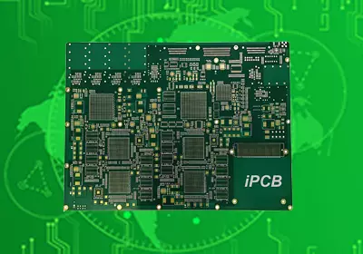
More than just a circuit carrier—IC Substrate is the unsung hero powering the world’s most advanced electronics, bridging bare semiconductors and PCBs to unlock breakthroughs in speed, miniaturization, and reliability. Designed for Flip Chip (FCBGA), Wire Bond BGA (WB-BGA), and Chip Scale Packages (CSP), this precision-engineered component doesn’t just meet industry standards—it redefines what’s possible for high-performance computing, automotive innovation, and 5G connectivity.

IC Substrate
Tailored Materials That Deliver Real-World Results
Every material in our IC Substrate is chosen to solve unique technical challenges, turning specs into tangible value:
ABF (Ajinomoto Build-up Film): The gold standard for speed and miniaturization. With a ultra-low CTE (≤9.8 ppm/℃) and dielectric constant of 3.48±0.1@1GHz, it enables ultra-dense circuit layouts—critical for shrinking smartphone SoCs and cramming more power into AI GPUs. Its 8/11 μm fine-line routing? That’s what makes your favorite devices slimmer and smarter.
BT Resin: Versatility meets dependability. Boasting a Tg≥182℃ and CTE of 13.2–16.8 ppm/℃, it’s the go-to for general-purpose WB-BGA/CSP packages. Whether powering consumer electronics or industrial sensors, its stable dielectric performance (4.1±0.1@1MHz) ensures consistent signal integrity, day in and day out.
Ceramic Substrates (AlN/Si3N4): The heat management game-changer. With AlN offering thermal conductivity up to 178 W/(m·K) and Si3N4 delivering bending strength≥780 MPa, it solves the overheating challenges of 5G RF modules and high-power industrial chips. No more compromising performance for durability—this substrate handles both.
Precision Engineering That Defines Reliability
Every detail of our IC Substrate is optimized to perform when it matters most:
Layer Flexibility: From standard 2–14 layers (perfect for WB-BGA/CSP) to high-density 6–22 layers (built for server CPUs and AI accelerators), we scale to match your design’s ambition.
Slim Yet Strong: Board thickness ranges from 0.14–1.9 mm (customizable up to 2.9 mm) with ultra-thin dielectric layers (13–46 μm)—ideal for devices where space is at a premium. Copper thickness (11–36 μm for signals, 67–103 μm for power) ensures it handles both delicate data and high-current delivery without breaking a sweat.
Surface Finishes That Last: Primary ENEPIG (Ni 2.8–4.8 μm / Pd 0.09–0.24 μm / Au 0.04–0.09 μm) fights corrosion and ensures rock-solid wire bond adhesion. Need something specific? Optional immersion tin, OSP, or hard gold finishes adapt to your assembly needs—whether for high-plug RF contacts or short-term storage.
Performance That Stands Up to the Elements
This isn’t just a substrate—it’s a workhorse built for harsh environments and nonstop operation:
Fine-Line & Microvia Innovation: Laser-drilled microvias (53–142 μm) and 8/11 μm line/space unlock Chiplet and HBM stacking capabilities, letting you pack more processing power into smaller spaces.
Impedance Control You Can Trust: ±4.8% tolerance (100Ω for DDR5, 85Ω for PCIe 5.0) eliminates signal distortion, so high-speed data moves seamlessly—critical for data center servers and 5G base stations.
Tough as Nails: Copper pillar thermal vias (Φ0.24 mm) keep temperatures in check, while warpage≤0.48% (for boards ≥0.5 mm) and peel strength≥1.15 N/mm ensure it survives assembly and years of use. It even endures -55℃~155℃ thermal cycles (1050 cycles, no delamination)—perfect for automotive ADAS systems that face extreme heat, cold, and vibration.
Powering the Technologies That Shape Tomorrow
Our IC Substrate isn’t just for today’s devices—it’s fueling the innovation behind smarter cars, faster data centers, and more connected devices:
High Performance Computing (HPC): 6–22 layer FCBGA substrates drive server CPUs and AI GPUs, making real-time data processing and AI training possible.
Automotive Electronics: AEC-Q200 compliance means it’s built for ADAS SoCs and in-vehicle radar—keeping drivers safe with reliable performance in every weather condition.
Consumer Electronics: ABF-based substrates shrink smartphone SoCs and power wearables, turning “impossible” miniaturization into reality.
5G/6G Communication: Ceramic substrates reduce signal loss in high-frequency RF modules, ensuring faster, more reliable connectivity for the next wave of wireless tech.
Product: IC Substrate
Material:
Core: ABF (Tg≥185℃, CTE≤9.8 ppm/℃); BT resin (Tg≥182℃, CTE13.2–16.8 ppm/℃); Ceramic (AlN:138–178 W/(m·K), Si3N4:≥780 MPa)
Prepregs: 22–47 μm,resin content 31–37%
Quality standard: IPC-4101F, AEC-Q200, UL94 V-0, RoHS 3.0
Dielectric constant:
ABF: 3.48±0.1@1GHz; BT resin: 4.1±0.1@1MHz; Si3N4: 3.78±0.1@10GHz
Layers: Standard 2–14 layers (WB-BGA/CSP); High-density 6–22 layers (FCBGA)
Thickness:
Board: 0.14–1.9 mm (max 2.9 mm custom); Dielectric:13–46 μm
Copper thickness:
Inner/Outer:11–36 μm (0.32–1.05 oz); Ultra-thick:67–103 μm (1.95–3.0 oz)
Surface technology:
Primary: ENEPIG (Ni2.8–4.8μm/Pd0.09–0.24μm/Au0.04–0.09μm)
Options: Immersion Tin (1.2–2.5μm), OSP (0.14–0.38μm), Hard Gold (0.07–0.26μm)
Special requirements:
Fine-line: Min L/S 8/11 μm, microvia 53–142 μm
Impedance: ±4.8% (DDR5:100Ω, PCIe5.0:85Ω)
Thermal/Mechanical: Φ0.24mm thermal vias, warpage≤0.48%, peel strength≥1.15N/mm
Environmental: -55℃~155℃, 1050 cycles no delamination
Application:
HPC: Server CPUs, AI GPUs; Automotive: ADAS SoCs; Consumer: Smartphone SoCs; 5G: RF modules
iPCB Circuit provides support for PCB design, PCB technology, and PCBA assembly. You can request technical consultation or quotation for PCB and PCBA here, please contact email: sales@ipcb.com
We will respond very quickly.