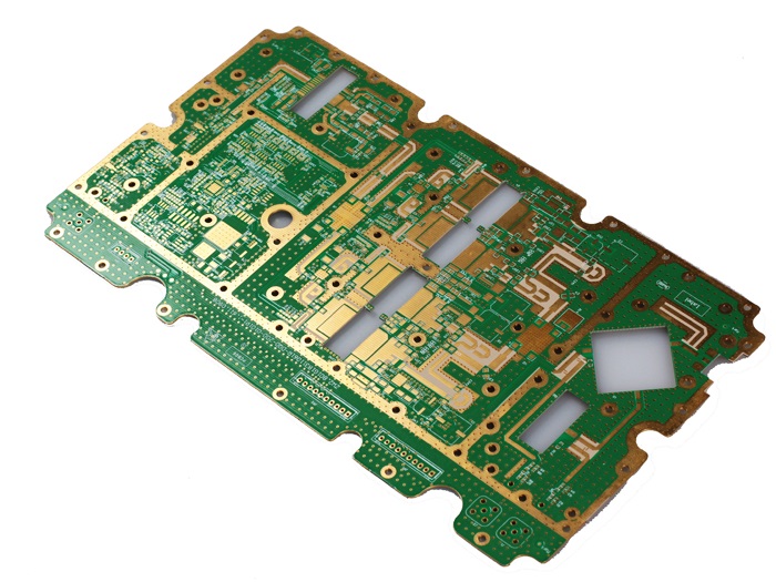
The backbone of modern industrial, telecommunications, and high-power electronics often requires a structure far exceeding the conventional circuit board. This structure is the large PCB. This specialized category of PCB is defined not merely by its physical size—frequently surpassing standard working panel dimensions—but by the significant engineering complexities it introduces.
The demand for large PCBs is driven by the necessity to consolidate high component counts, manage extensive power distribution -networks (PDN), and maintain system integrity across expansive surfaces. This makes them indispensable for high-density and high-power applications where reliability is absolutely non-negotiable.

large PCB
The Three Major Hurdles of Large PCB Design
Scaling a circuit design into a large PCB requires tackling inherent mechanical, thermal, and electrical physics challenges that intensify exponentially with the increased area. Failing to address these issues leads directly to manufacturing complications and premature product failure.
1. Mechanical Integrity and Warpage Control
The most critical initial challenge is managing the board's dimensional stability. A large area dramatically increases the board's susceptibility to warpage and twist during the high-temperature lamination and assembly processes. This deformation can compromise component soldering or even fracture critical connections. To effectively mitigate this risk:
---Stack-up Symmetry: Designers must ensure a perfectly symmetrical layer stack-up around the board's central plane, precisely balancing copper distribution to equalize internal stresses.
---Low-CTE Materials: Utilizing base materials with a low Coefficient of Thermal Expansion (CTE), such as specialized high-Tg FR-4 or polyimides, minimizes the dimensional change and strain caused by thermal cycling.
The structural requirements for a high-reliability large PCB necessitate meticulous attention during the initial material and stack-up definition phase to ensure flatness throughout its operational life.
2. Thermal Management at Scale
Heat removal becomes less efficient as board size increases, increasing the difficulty of avoiding localized hot spots and thermal gradients. Effective thermal solutions must be integrated into the board structure itself:
---Heavy Copper Layers: Using internal layers with copper weights of 3 ounces or more significantly improves lateral heat spreading and reduces resistive losses across the PDN.
---Thermal Vias: Dense arrays of thermal vias are mandatory to create a low-resistance path, efficiently drawing heat from high-power components down into the internal copper planes, which act as large internal heat sinks.
3. Signal and Power Uniformity
Across the large format, the intrinsic length of electrical paths is increased, amplifying transmission line effects. Long traces risk signal degradation, reflections, and crosstalk. Simultaneously, the Power Distribution Network (PDN) must maintain low impedance and uniform voltage across the entire surface to prevent excessive voltage drop (IR drop) and ground bounce. This challenge mandates precise impedance control on all high-speed lines and optimized, strategic placement of decoupling capacitors across the vast surface area.
Manufacturing Solutions for Large Format
Successfully fabricating a large PCB requires specialized equipment and stringent process controls that far exceed standard manufacturing capabilities.
1. Equipment and Process Requirements
Handling and processing oversized panels demands significant capital investment from the manufacturer:
---Lamination and Pressing: large PCBs require oversized, specialized hydraulic presses to ensure perfectly uniform pressure and temperature across the entire panel during the bonding process. This prevents internal voids, resin starvation, and delamination.
---Inspection and Testing: Wide-format Automated Optical Inspection (AOI) machines are necessary for high-resolution scanning of vast copper patterns. Furthermore, the immense volume of test points mandates complex, dedicated E-Test fixtures (bed-of-nails) for fast and comprehensive electrical verification. The successful fabrication of a large PCB heavily relies on these high-capacity, high-precision tools.
2. Layer Registration and Plating Precision
Achieving precise layer-to-layer alignment on high-layer-count boards is a geometrical imperative. Any minor registration error is magnified over the board's length. Modern fabrication employs sophisticated optical targeting and automated pin lamination to achieve the sub-mil accuracy needed for inner layer connections.
Crucially, the thickness of these boards results in a high aspect ratio for the through-holes (vias). Plating copper uniformly into these deep, narrow barrels requires advanced chemical processes and carefully managed "throwing power" to ensure the copper plating is thick and reliable at its center—the most critical point for long-term reliability against thermal stress and cycling.
3. Quality, Yield, and Cost Focus
Due to the increased material cost and the overall complexity of the manufacturing chain, the cost of a large PCB is intimately tied to its manufacturing yield. A defect in any one of the dozens of process steps can result in scrapping an entire, high-value panel. This necessitates:
---Rigorous E-Test: Every single net must be tested for shorts and opens before final assembly.
---Process Monitoring: Constant, real-time control and data logging of chemical baths, pressure cycles, and etching rates are essential to maximize the yield of these high-value components.
The large PCB remains the essential technological cornerstone of many mission-critical systems today. Ready to move your complex electronic system from concept to reliable hardware? Contact our engineering team today to leverage our expertise in Large PCB design optimization and manufacturing, ensuring your high-value project scales successfully and reliably.