A Trustworthy PCB and Electronic Manufacturing Enterprise! Contact Us


What is a pcb circuit board? PCB circuit board, also known as a printed circuit board, is the core component of an electronic device used to connect electronic components. It replaces traditional manual wiring with pre-designed conductive lines, making circuits more compact and reliable. In short, PCB is like the ‘skeleton’ and ‘blood vessels’ of electronic products, supporting components and transmitting signals and electricity.
What does pcb stands for? PCB is a kind of conductive copper foil patterned by laying on the surface of insulating materials (such as glass fibre, epoxy resin, etc.) to form an electrical connection between electronic components of the board. Its main function is to realise the electrical connection between electronic components through these copper foil lines and to support the components to be fixed on the board.
The core function of the printed circuit board is to realise the transmission and distribution of electrical signals, and to send power and control signals to each electronic component. Its working principle can be simply understood as follows: through the conductive copper foil and different circuit paths, the various electronic components are connected to achieve the flow of current and the transmission of signals.
For example, in the computer motherboard, the printed wiring board not only connects the processor, memory, graphics card and other major components,but also through the power supply circuit for their power supply, and through the control signals to co-operate with the work of the various parts. The stability and reliability of the printed wiring board directly affects the performance of the entire electronic device.
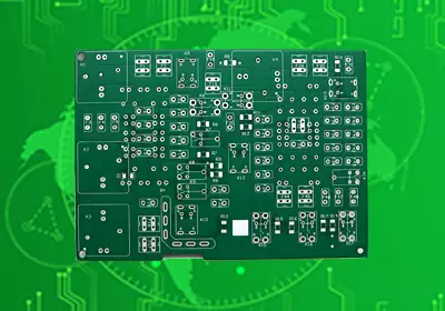
Structure of PCB circuit board
At its most basic level, a pcb circuit board is a flat, hard piece of insulating material with thin conductive structures attached to one side. These conductive structures form geometric patterns, including rectangles, circles, and squares. The long, tin rectangles serve as interconnects (i.e., wire equivalents), while the various shapes serve as connection points for components.
In general, PCB boards consist of the following main components:
Substrate: usually made of glass fibre or epoxy resin, providing mechanical support and insulation.
Conductive layer: made of copper foil, responsible for transmitting current and signals.
Soldermask layer: protects the copper foil of the board from oxidation and prevents short circuits.
Character layer: Marks the location of components on the circuit board for ease of assembly and maintenance.

PCB circuit board Stack-up
Classification of PCB circuit boards
Classification according to the number of circuit layers
Printed circuit boards can be divided into single-sided, double-sided and multilayer boards according to the number of circuit layers. Common multilayer boards usually have 3 to 6 layers, while the complex structure of the multilayer board can reach more than a dozen layers.
Single-sided pcb board
Single-sided pcb board is the most basic form of printed circuit boards, with electronic components concentrated on one side of the circuit board and wires arranged on the other. Since the wires are only present on one side, this type of board is called a single panel. Since the wiring can only be done on one side, there are more limitations in the circuit design, which cannot be cross-wired and can only take a wire-wrap path, so early circuits mostly used this type of board.
Double-sided pcb board
Double-sided pcb board have wiring paths on both sides. In order to realise the electrical connection between the two sides, it is necessary to complete it by means of vias. Vias are small holes plated with metal on the board that connect the circuits on both sides of the board. Since the wiring area of a double-sided board is twice as large as a single-sided board, and circuits can be cross-utilised on different sides, it is possible to meet the needs of more complex circuit designs than single-sided boards.
Multilayer pcb Board
Multilayer pcb boards use multiple layers of single- or double-sided wiring boards to increase the wiring area by sandwiching insulating layers between each layer and bonding them together. The number of layers in a multilayer board, i.e. the number of independent wiring layers, is usually even, including the two outermost layers. This design allows for denser and more powerful circuits.
Classification by Substrate Type
Printed circuit boards can also be classified as flexible PCBs, rigid PCBs and rigid-flexible PCBs based on the type of substrate.
Flexible PCB is made of flexible substrate with good bending performance, which facilitates the assembly of complex electrical components. They are widely used in aerospace, military, mobile communications, notebook computers, computer peripherals, PDAs and digital cameras.
Rigid PCB
Rigid circuit board using paper-based (mostly used for single-panel) or glass cloth-based (mostly used for double-sided and multilayer boards), pre-impregnated with phenolic or epoxy resin, the surface of the adhesion of one or two layers of copper-clad laminate made of cured by lamination. Rigid PCB material is hard and not easy to bend, can provide solid support for electronic components.
Rigid-Flex PCB (Rigid-Flex PCB)
Rigid-flex PCB integrates rigid and flexible areas on the same board, and is made by combining rigid and flexible boards through lamination technology. It combines the support of rigid PCBs and the flexibility of flexible boards to meet the needs of complex three-dimensional assemblies.

Rigid-Flex PCB
Classified by PCB material
Metal substrate: good thermal conductivity, suitable for high-power equipment.
Paper substrate: low cost, phenolic resin as the binder, wood pulp fibre paper as the reinforcing material for the insulation laminate material, the relative density is small, can be punched processing, but the working temperature is low, humidity resistance and heat resistance is slightly lower, applicable to general electronic products.
Synthetic resin substrate: such as FR-4 epoxy resin glass fibre cloth board, high operating temperature, its own performance by the environmental impact of small, in the processing process has a great deal of superiority, suitable for high-end electronic products.
Ceramic substrate PCB: Aluminium oxide (Al2O3) or Aluminium Nitride (AlN) ceramic substrate as the substrate material, with excellent electrical insulation properties, high thermal conductivity characteristics, excellent soft brazing and high adhesion strength, widely used in areas requiring high thermal conductivity and high reliability.
The detailed process of PCB circuit board production
1. Opening (CUT) - The original copper-clad board will be cut according to the design requirements to meet the production specifications of the initial board form.
2. Drilling - According to the characteristics of the pcb circuit board, accurately drill the holes of the required specifications in the preset position.
3. Copper sinking - A thin layer of copper is chemically deposited uniformly on the walls of the insulating holes.
4. Pattern transfer - The designed film pattern is precisely transferred to the surface of the pcb circuit board.
5. Pattern Plating - Thicken the copper layer on the guide holes and line parts to ensure that the copper thickness required for the finished product is achieved.
6. Fading treatment - Using sodium hydroxide solution to remove the anti-electroplating film from non-line covered areas, exposing the copper layer.
7. Etching - Remove the copper in the non-circuit part by chemical etching to form a complete circuit pattern.
8. Green Coating - The green oil pattern is transferred to the printed circuit board to protect the circuit and avoid solder bridge short circuits during soldering.
9. Screen Printing Characters - The screen printing process is used to accurately print the required text logos and information.
10. Surface treatment - Surface protection treatment of the exposed copper layer to prevent oxidation and corrosion. Commonly used methods include spray tin, immersion gold, OSP (organic protective film), immersion tin, immersion silver, and nickel - palladium - gold and electroplated gold fingers.
11. Shape Processing - Using CNC machining equipment to cut the PCB circuit board into the shape and size required by the design.
12. Testing Stage - After completing the shape processing, strict circuit testing is carried out to ensure that there are no short circuits or other functional defects.
13. Final Inspection Process - The final PCB circuit board is fully inspected, covering appearance quality, dimensional accuracy, aperture size, board thickness and labelling information to ensure that the product meets the standard requirements.

PCB circuit board production
What are pcbs use for?
1. Communication Equipment - PCB circuit boards play a vital role in communication equipment and are widely used in telephones, mobile phones, radios, satellite communication systems and other data transmission equipment to provide a reliable signal transmission path and ensure the accuracy of data transmission.
2. Medical Equipment - Medical equipment requires a high degree of precision and reliability, and PCB meet these needs. They are widely used in medical diagnostic instruments, monitoring equipment, surgical instruments, and implantable devices to ensure proper functioning of the equipment and patient safety.
3. Industrial Controls - PCB board play a central role in industrial automation systems, and are used in robots, CNC machine tools, and production line automation equipment for precision control and efficient operation.
4. Automotive Electronics - Modern automobiles are equipped with a large number of printed circuit board, such as engine control units, body control modules and airbag control systems, supporting a number of electronic functions of the vehicle.
5. Household Appliances - Printed wiring board is also widely used in a variety of home appliances, such as televisions, refrigerators, washing machines and air conditioners, etc., to enhance the performance and intelligence of home appliances.
6. Instrumentation - In scientific research and industrial production, PCB Board provide stable signal transmission for all kinds of precision instruments to ensure the accurate collection and recording of measurement data.
7. Aerospace - The aerospace field requires high precision and reliability of equipment, printed wiring boards are used in aircraft, rockets, satellites and other equipment to support complex control and monitoring functions.
8. Computers and Servers - PCB circuit board is used in a large number of computer and server systems to ensure stable and efficient signal transmission and to support high-speed data processing and transmission.
9. Internet of Things Devices - With the development of the Internet of Things, PCB being used in expanding applications in smart homes, smart cities and environmental monitoring, which greatly facilitates people's daily lives.
In addition, PCB circuit boards are also widely used in military defence, energy field and LED lighting and many other industries, playing an important fundamental role.

PCB circuit board