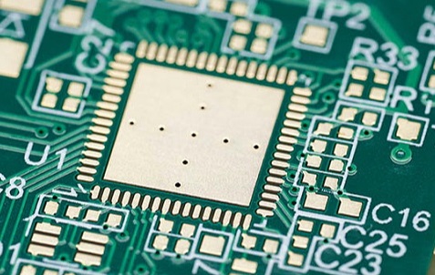
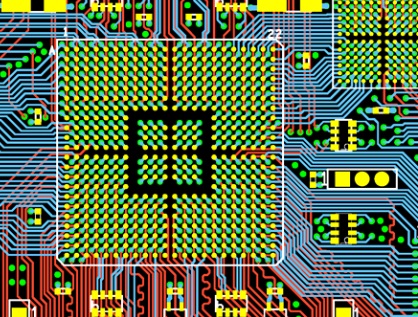
There are three main categories of pcb board layers: structural layers, functional layers, and conductive layers.
PCBs have different structural layers such as substrate, copper, solder mask, and silkscreen. Each layer of a PCB plays a specific role.
To make a PCB, these layers are stacked on top of each other. Adhesives hold them in place. The most important are the copper layers. They are placed between insulating layers. Hence, a PCB layer is like a single layer in a sandwich.
Regarding the conductive layers, the number of PCB layers is usually the number of copper layers in a PCB. To accommodate complex circuit designs, multiple layers are required.
However, there are eight different functional layers. We will discuss these layers in the next few sections.
Each layer in a PCB serves a unique purpose. The substrate layer makes the PCB strong. Copper helps connect electrical components. On the other hand, the solder mask protects the traces from damage. Lastly, the silkscreen helps us know which part is which.
Without these layers, electronic devices will not work properly. Hence, each layer is very important for the working of a PCB.

pcb board layers
pcb board layer 1:Substrate Layer
The substrate layer is the foundation of the PCB. It provides a strong base for all its components. You will find it on the bottom of the PCB. It holds all the elements together.
The substrate is usually made of fiberglass (FR4). It is tough and rigid, ensuring the stability of the PCB. Although flexible PCBs may be made of plastic (Kapton), some may use epoxy. However, fiberglass (FR4) is the best material for making high-quality circuit boards.
pcb board layers 2: Copper Layer
The copper layer is a thin piece of copper foil that is attached to the board after heating. It is located just above the substrate layer. The copper layer is essential for conducting electricity.
Different PCBs have different numbers of copper layers. Single-sided PCBs have only one layer of copper and are usually used for simpler electronic devices.
Double-sided, on the other hand, have copper on both sides. They usually use vias to connect the top and bottom layers. Therefore, they can handle tighter trace routing. This feature is very convenient for connecting circuits across the board.
Note that thicker copper layers are popular for handling high power.
pcb board layers 3:PCB Layer #3 Solder Mask
The solder mask is a protective coating applied to the surface of the PCB. It is usually green in color and covers the copper traces on the PCB. It acts like a shield, preventing the copper traces from touching anything that could cause damage.
Once the copper layer is in place, you can add the solder mask. This layer also insulates the copper, preventing it from touching other metals.
The solder mask is usually made of liquid epoxy. For coloring, this liquid comes with a green pigment.
pcb board layers 4:Silkscreen or Coverlay
The silkscreen layer, also known as the coverlay, is the outermost layer of the PCB. It contains letters, numbers, and symbols, just like labels on a map.
The silkscreen usually acts as your guide. It shows you which part on the PCB is connected. With labels and symbols, it is easier to know where the LED or pin is connected.
Multilayer pcb board layers:
1. A brief introduction to Core and PP
The Core is the core component of the PCB multilayer board. Its two surface layers are covered with copper foil, which can be used as conductive layers such as signal layer, power layer, and ground layer. The upper and lower surface layers of the Core are filled with solid materials, which have good mechanical strength and electrical properties. PP is a semi-solid resin material with no copper foil on the surface, which plays a filling role in the PCB. PP is slightly softer than Core, so when making multilayer boards, Core and PP need to be used together. Generally, PP should be used as a filler between two Cores.
2. Prerequisites for stacking structure design
When designing the stacking structure of a PCB multilayer board, the following information needs to be obtained in advance: Total number of layers of a single board: including the number of signal layers, power layers, and ground layers. The determination of these layers needs to be roughly estimated based on the size of the single board, the scale of the single board (such as the number of signals, the type of power supply, etc.) and the requirements of EMC.

pcb board layers
Single board thickness: The thickness of a single board is related to the width of the rail, and also depends on factors such as the total number of layers. For example, the thickness of a single board with less than 14 layers can be selected as 1.6mm, while the thickness of a single board with more than 16 layers must be more than 2mm. In some designs, due to the limitation of the width of the rail, and the total number of layers of the single board cannot be reduced, the area where the single board contacts the rail can be thinned by chamfering.
Target impedance: Considering signal integrity, impedance matching is required on the signal transmission path. Generally, the impedance of a single-ended signal to ground is 50Ω, while the impedance between differential pair signals is 100Ω.
Different pcb board layers have different roles.