When you design a PCB, you follow important steps. First, you define what you need. Next, you draw schematics. Then, you build the layout. After that, you check your work. Last, you get files ready for production. You can use easy tools like EasyEDA, KiCad, or LibrePCB. Allan Knox is a Senior PCB Design Engineer. He says Eagle and KiCad are good for new users. These tools have open-source features. Many beginners make mistakes when designing PCBs:
Not watching trace width and spacing
Forgetting about via sizes
Not thinking about power and ground plane layouts
Not designing for manufacturability
Putting decoupling capacitors in the wrong place
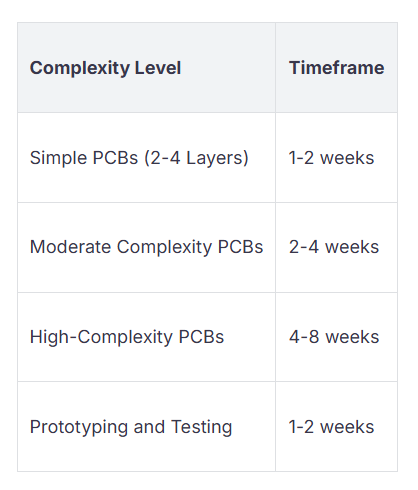
You should plan your project well and check each step. A simple PCB project usually takes one to two weeks.

Make sure you know what your project needs before you begin. This helps you not make mistakes and saves time later.
Pick good PCB design software like EasyEDA or KiCad. These programs have easy features for people new to designing.
Always do a Design Rule Check (DRC) before making your board. This step finds mistakes and makes sure your board works right.
Choose parts carefully by looking at datasheets. Make sure the parts fit your design and are easy to get.
Build a prototype and test your design before making many boards. This helps you find problems early and makes your product better.
You should make a clear plan before you start. Think about what your project needs. Ask yourself what the board will do. Think about how big it should be and where it will be used. For consumer electronics, focus on these important things:
Know what your project is for and what it needs.
Pick the right size and shape for your device.
Choose materials that fit your budget and work well.
Plan how to keep the board cool so it does not overheat.
Make sure power stays steady for good performance.
Keep signals clear for fast data movement.
Build your board to last and work well.
Make your design simple to build in a factory.
Follow safety rules and industry standards.
You also need to set some basic details. Decide how big the board will be. Pick how many layers it needs. Choose the material, thickness, copper weight, and surface finish. Set rules for trace width, spacing, and drill sizes. Write down power and signal needs, where the board will be used, and how you will test it. Make a timeline with goals to help you stay on track.
Tip: Write down all your needs before you begin. This helps you avoid mistakes and saves time later.
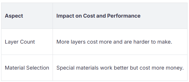
Learn about how a PCB is built before you start. A PCB has copper layers and insulation. More layers cost more and are harder to make. The table below shows how layers and materials change your design:

Most boards use FR4 because it is good and not too expensive. Fancy materials cost more but work better in tough places.
How you put layers and traces together matters for signals. Good spacing stops signals from mixing and causing problems. Put parts where the schematic shows and keep paths short. Beginners can find easy guides online to learn PCB basics. These guides help you feel sure when you design a PCB.
You need a clear schematic before you design a PCB. The schematic is like a map for your board. It shows every part and how they connect. You use this drawing to help with layout and checking later. If you skip or rush this, you might make mistakes. Mistakes can cause your board to not work.
First, open your schematic tool. EasyEDA, KiCad, LibrePCB, and Autodesk Fusion Electronics help you draw diagrams. These tools let you put symbols for each part. You connect them with lines and organize your design. EasyEDA links to LCSC, so you can find parts fast. KiCad has open-source features and a helpful community.
Pay close attention when you draw your diagram. Show every connection clearly. Label each part and wire. If you use outside parts, check their symbols and footprints. Sometimes, you must change footprints to fit your design.
Tip: A correct diagram helps your PCB work well. A good schematic helps you find problems early and keeps things neat.
You may face some common problems:
Making sure footprints and symbols are correct
Problems with special footprints
Needing changes for your design
A good schematic helps you:
See how your circuit works
Find problems before building
Test and fix your PCB after making it
Spend time making your schematic clear and right. This helps your PCB work well.
Pick the right parts for your project. Each part should fit your design and work with others. Start by reading datasheets. Check electrical, mechanical, and environmental details. Look for parts that match your needs and are easy to buy.
Here are important things to help you pick good parts:
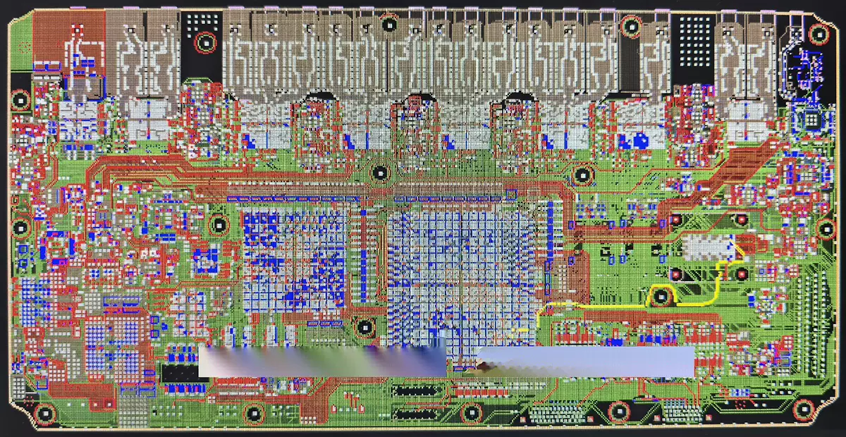
After finalizing component selection, turn your schematic into a physical PCB layout—this is where your design becomes tangible. Start by placing components strategically: group functional blocks (e.g., power circuits) together, leave space for soldering/assembly (to avoid the "poor manufacturability" mistake), and align parts to match the schematic’s logic.
Pay close attention to trace width/spacing (a top beginner error) and via sizes: use the design rules you set earlier to ensure traces handle current safely and vias fit component leads. For high-speed signals, keep paths short and minimize sharp bends to reduce interference. Also, prioritize power/ground planes (instead of just traces)—this fixes the common issue of neglecting power stability and improves signal integrity.
Never skip post-layout checks—they prevent costly production errors. First, run a Design Rule Check (DRC) in your tool (e.g., KiCad): it flags issues like incorrect spacing, missing connections, or mismatched vias.
Next, do a manual cross-check between the schematic and layout (to catch misplaced decoupling capacitors, another beginner mistake). For complex designs, use signal integrity simulations to test high-speed path performance—this ensures your board works as intended.
Once your design passes checks, generate the files manufacturers need:
Gerber files: These include layer details (copper, solder mask, silkscreen) — most tools (e.g., EasyEDA) have built-in exporters for this.
Drill files: Specify the size/location of all holes (vias, component leads).
Double-check the manufacturer’s requirements (e.g., minimum trace width) before sending files—this avoids "unmanufacturable design" issues.
Order a small prototype batch (most suppliers offer low-cost small runs) — this aligns with the 1–2 week prototyping timeline noted earlier. Assemble components and test the board: check power stability, signal functionality, and heat buildup.
If you find issues (e.g., a narrow trace causing overheating), revise the layout/schematic and re-prototype. This iterative process ensures your final design is reliable before full production.
By following these steps—from layout to testing—you’ll sidestep common beginner mistakes and create a functional PCB. Remember: thorough planning and checks (as highlighted in the key takeaways) are the backbone of successful PCB design.

PCB Design