A Trustworthy PCB and Electronic Manufacturing Enterprise! Contact Us


1. To ensure high-quality results in PCB manufacturing, which processes are most critical in the photoresist pcb board process?
When focusing on the photolithography process, we always start from the beginning: surface preparation, film application, exposure, and finally development. Of course, if deemed necessary, we also focus on other processes such as photoresist stripping, etching, or even plating applications. Each step is equally important to the next. All these processes should have daily checks and protocols to ensure consistency and repeatability. However, if one must choose the most critical step, surface preparation is undoubtedly paramount. Just as building a house requires a solid foundation for success.
2. What are the latest developments in photoresist materials or processes significantly impacting PCB manufacturing?
The most significant advancements in this field focus on high-resolution, high-adhesion, 1 mil (25μm) thin photoresists for IC substrates, along with various higher technical demands. Such photoresists will enable etch heights below 1:1 to achieve high resolution and small feature sizes while still providing sufficient resist height for plating applications. For post-etch feature sizes, some customers target finished products within the 12–20μm range.
3. What are the most common defects encountered in photoresist processes, and what are typical causes?
In terms of sheer volume, I believe the most prevalent defects are open circuits and short circuits. In every facility I've visited, these two defects consistently rank as the top photoresist issues discussed. When defining open and short circuits, it is always necessary to first determine whether the discussion pertains to inner layer processing or outer layer (overlay) processing. I consistently request customers to categorize these defects into two groups, as making too many generic changes across the process will only exacerbate issues. Many inner layer opens can be attributed to cleanliness in the imaging and film application areas, as well as certain pre-cleaning process lines. For sustained high yield, a true cleanroom equipped with cleanroom equipment, protocols, and proper attire (including booties, coveralls, caps, and masks) is essential for most modern technology requirements. Sticky machines or manual rollers are ideal for pre-lamination cleaning and for keeping polyester film free of debris post-lamination and pre-exposure. Maintaining the cleanliness of exposure equipment and its processing tables/trays is also critical. Incoming and used substrate masking plates should always be inspected to ensure no visible dents or scratches. These imperfections can cause resist adhesion issues, manifesting as adhesion loss—a primary failure mode that ultimately leads to open or short circuits. Short circuits in inner layers can result from multiple causes—insufficient etching or development leading to poor etching. They may be triggered by debris on the surface or beneath the photoresist, causing exposure issues that result in adhesion loss or photoresist lifting and reduction in unintended areas. Handling damage or transport damage can also cause photoresist lifting and migration. Outer layer open circuits and short circuits are not necessarily dependent on the cleanroom, but cleanroom standards should be equally important as for inner layers. Adhesion loss during outer layer processes can cause plating short circuits, while inadequate filtration during pre-plating cleaning can lead to particle redeposition on the surface, resulting in short circuits or open circuits. Similarly, handling damage can also cause issues. Due to resist-related issues, resist peel shorts or trapped/squeezed resist will be considered shorts, but these are typically associated with plating and resist peel or chemical solution content issues specifically affecting photoresist. The primary and most common areas for defects are: the duration of photoresist exposure on copper (rule of thumb: aim to complete masking and stripping within 72 hours), surface preparation for overlay processing, and maintaining cleanroom control.

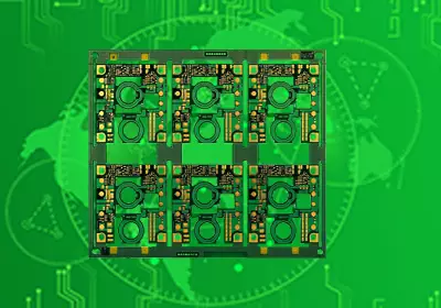
photoresist pcb board
4. What challenges does the photoresist process face when handling complex materials such as PTFE or flexible substrates? What circumstances might prompt manufacturers to change their resist products?
These materials require optimal adhesion. The first challenge that comes to mind is when customers experience adhesion loss or resist cracking during the photoresist process. Softer resists with high adhesion are ideal. The obstacle will depend on the manufacturer's capabilities. Flexible substrates are more susceptible to handling damage, dents, and scratches. Resists are needed that can compensate for any such potential issues and compensate for inadequate material preparation prior to coating.
5. How can photoresist adhesion issues on PCB surfaces be addressed, particularly for multilayer boards or boards with challenging materials?
Adhesion loss is always a concern. The first step is to review process controls and surface treatments applied. For example, is surface preparation chemical or mechanical, or is no treatment applied at all? Ideally, surfaces should always be treated to create an optimal environment for resist adhesion and conformality. However, some customers may lack these capabilities, or materials may be unsuitable due to handling constraints (soft flexible materials), or grain/surface characteristics cannot be altered (RF applications). In these worst-case scenarios, for RF applications, non-etch-based adhesion promoters are still recommended, or for flexible materials, improved handling systems should be adopted.

photoresist pcb board
6. How has photoresist technology evolved to address the challenges of smaller, finer PCB features? What new technologies or methods are being researched and developed in photoresist pcb board development to enhance performance and reduce defects in PCB manufacturing?
Photoresist technology has made significant strides over the years. Today, we have exposure heads with multiple exposure units as small as 6μm—truly remarkable when you consider it. The resist itself is at the forefront of fine-feature and high-resolution PCB technology. We are now handling customer-plated feature sizes below 1 mil (25μm), which is not an easy process. The photoresists we test and sell for such PCBs can achieve significantly lower heights than 1:1 photoresists. This means, for example, we can print 15μm traces with 25μm photoresist height spacing while still allowing room for plating as required by the design. However, even at this cutting-edge level of photoresist technology, the technical capabilities of the latest available exposure equipment, vacuum film application techniques, and track vertical development must be considered to enhance yield and capability. Furthermore, given the size of the fine features and the materials used, the importance of cleanliness and handling cannot be overstated.