A Trustworthy PCB and Electronic Manufacturing Enterprise! Contact Us


Pre-sensitisation is a method of processing PCBs (printed circuit boards) that involves the use of ultraviolet light exposure. Presensitized pcb board with ultraviolet light is an interesting and unique way to handle your DIY electronics projects.
However, it involves many steps!
Introduction to presensitized pcb board
What is the significance of pre-sensitising PCBs? The main advantage of pre-sensitisation is that it is more precise than other PCB processing methods (such as toner transfer).
If you are an electronics enthusiast who enjoys creating unique projects, making pre-sensitised PCBs can be a lot of fun.
Another major benefit of pre-sensitised PCBs is that this process is very cost-effective. The pre-sensitisation process for PCBs eliminates manufacturing steps, thereby reducing costs, allowing you to pursue your creative passion without worrying about budget constraints!
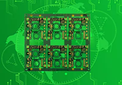
What exactly is a presensitized pcb board?
A pre-sensitised PCB is a special type of PCB where the board's surface is coated with a unique photosensitive material. This pre-sensitised PCB allows you to easily apply unique custom designs by using UV transfer (or ‘etching’) to transfer the image.
Presensitized pcb boards are similar to standard copper-clad PCBs, with the main difference being how the design is transferred to the board.

presensitized pcb board
Traditional (copper-clad) PCBs transfer images using the following methods:
* Toner transfer method
* Inkjet mask method
* Dry film photopolymer method
Using an innovative liquid film method.
Pre-sensitised PCB boards transfer images using the following method:
* Exposure to ultraviolet light
During manufacturing, a special photosensitive coating is added to the pre-sensitised PCB. The photosensitive coating is highly sensitive to light! The ‘release’ layer protects the unique photosensitive coating from accidental exposure. The peelable protective layer must be removed immediately before exposure to ultraviolet light!
PCB Preparation Process
Remember, printed circuit boards require a lot of effort, patience, and testing! Therefore, remember that mistakes may occur when printing PCBs for the first time using photosensitive PCBs. Therefore, creating multiple experimental boards when attempting any manufacturing tests for the first time may be a brilliant idea.
It is also a good idea to familiarise yourself with reliable PCB manufacturers so that you can use reliable components with confidence, and the supply chain will not be reduced, fade, or become an issue during production!
PCB Preparation
When using pre-sensitised PCBs, first carefully observe the thick grey film on both sides of the circuit board. This film is designed to protect the circuit board itself from UV radiation.
Remember, once you remove the film, the circuit board becomes highly sensitive to light, so do not remove the film until you are ready to expose it to UV light immediately!
Before removing the protective film, be sure to cut the circuit board according to the project specifications. PCBs and protective films are surprisingly durable, so there is no need to worry about damage. Cutting the PCB into a larger size than the pre-sensitised pattern may be a wise decision, as this extra space is very useful during the etching stage of the circuit board.
Now that your board is cut, it might be a better idea to prepare a second (or third) board so you can experiment with the exposure process and aim for the best results. Remember, practice makes perfect, and using pre-sensitised circuit boards for the first time may present challenges!
PCB Exposure
PCB exposure is typically done in an exposure box. An exposure box is simply a box containing a UV lamp. You can create your own custom exposure box or search for a pre-assembled box at your favourite electronics store. However, if you're a true electronics enthusiast, creating your own exposure box might be more fun.
The most important thing to remember is that if the glass on either side of the exposure box is dirty, those stains can easily transfer to the PCB during the exposure process!
Nothing is more frustrating than seeing ugly spots, specks, stains, or defects on a perfectly clean board. Therefore, there is no doubt that the glass and UV lamps inside the exposure box must be completely clean. Before starting the exposure process, you should wipe the glass of the exposure box with a microfibre cloth and neutral detergent to ensure the surface is free of contamination.
Additionally, please remember that when you remove the grey protective film from the pre-sensitised board, almost any light source will affect your board. Your circuit board is highly sensitive to light! Therefore, it is best to work in a relatively controlled area without strong light (except for the ultraviolet light in the exposure box, of course).
Once you have confirmed that the exposure box is clean and all additional strong light sources have been eliminated, it is time to remove the protective film from either side of the pre-sensitised board.
Now that the protective film has been removed from the desensitised circuit board, please remember not to touch the surface of the circuit board. The circuit board is highly sensitive, so please take care not to get it dirty or expose it to any sharp, bright light!
Carefully place the top and bottom of the pre-sensitised PCB artwork layer on the circuit board so that everything is perfectly aligned and centred. Once you are satisfied with the alignment, place the pre-sensitised board into the exposure box. Do not turn on the light!

presensitized pcb board
After placing the board in the exposure box, it is best to place a thin, flat piece of glass on top of the board. The reason for this is to ensure that the artwork layer can contact the surface of the board and that both the board and the artwork layer are flat.
Once you have confirmed that the artwork layer is fully aligned on the board and that the artwork is flat on the board, you can turn on the exposure light.
The time required for the exposure process will vary depending on the intensity of the light and the overall design of the exposure box. Typically, you can expect the exposure process to last between 1 minute and over 10 minutes! This variation is why experimentation is so important, and why we recommend making multiple copies of the circuit board!
Pre-sensitised PCB Conclusion Document
Advantages of manufacturing unique presensitized pcb board:
1. It offers a convenient technique for electronic DIY enthusiasts.
2. It may be a good method for creating unique PCB designs.
3. Steps in the manufacturing process can be eliminated, making it faster and cheaper.