A Trustworthy PCB and Electronic Manufacturing Enterprise! Contact Us


Product: Probe Card PCB
Material: Isola 370HR (Tg 180°C, Dk 4.04 @1MHz) or Rogers RO4350B (Dk 3.48 @10GHz) for high-frequency testing
Quality standard: IPC-6012, IPC-A-610, JEDEC JESD22
Dielectric constant: 4.0–4.5
Layers: 14–42 layers
Thickness: 1.8–4.8mm (tolerance ±0.15mm)
Copper thickness: Inner layers: 0.6–2.2oz (≈21–77μm); Outer layers: 0.9–2.0oz (≈31.5–70μm)
Surface technology: Hard gold plating (2.5–12μm) or ENIG (0.06–0.12μm gold) with nickel underlayer (3–6μm)
Special requirements: High-precision via placement (±6μm), depth-controlled drilling, metal cladding for structural stability
Application: 3nm/5nm logic chips, HBM3 memory modules, MEMS devices, automotive AI chips (AEC-Q200 compliant)
Semiconductor manufacturing demands ultra-precise signal transmission and durable probe contact when verifying 3nm/5nm chips, High-Bandwidth Memory (HBM), or MEMS devices. The Probe Card PCB emerges as a critical bridge between automated test equipment (ATE) and wafer test points, enabling defect detection before packaging — and slashing post-production failure costs by over 60%.
Core Advantages: Advanced Materials & Structural Design
Every Probe Card PCB is engineered with cutting-edge specifications to meet semiconductor testing rigor:
Base Material: Utilizes Isola 370HR (Tg 180°C, dielectric constant 4.0–4.5 @1MHz) for high-temperature test scenarios; optional Rogers RO4350B (dielectric constant 3.4–3.6 @10GHz) for RF/mmWave chip testing (e.g., 5G transceivers).
Layer & Thickness Flexibility: Supports 14–42 layers (tailored for high-pin-count ICs like AI accelerators) with a standard 2.0mm thickness (±0.15mm tolerance), upgradable to 4.8mm for heavy-duty probe arrays.
Copper & Surface Technology: Inner copper thickness ranges from 0.6oz (≈21μm) to 2.2oz (≈77μm) for optimal signal integrity; outer layers use 0.9–2.0oz (≈31.5–70μm) copper, paired with hard gold plating (2.5–12μm) or ENIG (0.06–0.12μm gold + 3–6μm nickel) to resist wear during repeated probing.
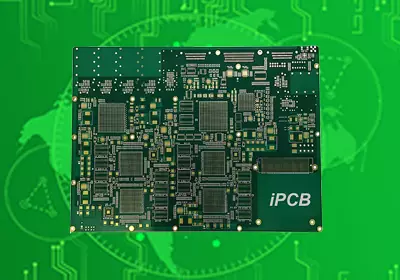
Probe Card PCB
Technical Performance: Enabling Nanoscale Testing
To validate advanced semiconductor nodes, the Probe Card PCB meets strict technical demands:
Impedance Control: Maintains 50Ω (single-ended) / 100Ω (differential pair) impedance within ±10% — critical for high-speed protocols like DDR5 and PCIe 6.0.
Precision Manufacturing: Features ±6μm via placement tolerance and depth-controlled drilling to ensure alignment with sub-30μm chip pads.
Thermal Stability: Integrates metal cladding and reinforced epoxy layers to prevent warping across ATE thermal cycles (-40°C to +150°C).
Industry Applications: Powering Semiconductor Innovation
The Probe Card PCB is essential for sectors relying on cutting-edge chips:
3nm/5nm Logic Chips: Tests billions of transistors in nodes like Apple M3 or AMD Ryzen 8000 using multi-thousand-pin probe arrays.
High-Bandwidth Memory (HBM3): Enables parallel testing of stacked memory dies to ensure 819GB/s+ data throughput for AI supercomputers.
MEMS & Automotive ICs: Validates MEMS sensors (gyroscopes, pressure sensors) and AEC-Q200-compliant automotive AI chips (e.g., NVIDIA DRIVE Orin) under extreme temperature and vibration.
Product: Probe Card PCB
Material: Isola 370HR (Tg 180°C, Dk 4.04 @1MHz) or Rogers RO4350B (Dk 3.48 @10GHz) for high-frequency testing
Quality standard: IPC-6012, IPC-A-610, JEDEC JESD22
Dielectric constant: 4.0–4.5
Layers: 14–42 layers
Thickness: 1.8–4.8mm (tolerance ±0.15mm)
Copper thickness: Inner layers: 0.6–2.2oz (≈21–77μm); Outer layers: 0.9–2.0oz (≈31.5–70μm)
Surface technology: Hard gold plating (2.5–12μm) or ENIG (0.06–0.12μm gold) with nickel underlayer (3–6μm)
Special requirements: High-precision via placement (±6μm), depth-controlled drilling, metal cladding for structural stability
Application: 3nm/5nm logic chips, HBM3 memory modules, MEMS devices, automotive AI chips (AEC-Q200 compliant)
iPCB Circuit provides support for PCB design, PCB technology, and PCBA assembly. You can request technical consultation or quotation for PCB and PCBA here, please contact email: sales@ipcb.com
We will respond very quickly.
