A Trustworthy PCB and Electronic Manufacturing Enterprise! Contact Us


What is SMT?
SMT stands for Surface Mount Technology, which is currently the mainstream component assembly technology in the field of electronic manufacturing. Its core is to directly solder small-sized SMD onto the surface of Printed Circuit Board, rather than the traditional THT method of inserting component pins into PCB holes. It has completely changed the development of miniaturization, lightweighting, and high integration of electronic devices. Almost all electronic products we use in our daily lives, such as smartphones, computers, smartwatches, and home appliances, rely on SMT technology to manufacture their circuit boards.
Electronic products pursue miniaturization, but the previously used perforated plug-in components cannot be reduced in size. At present, the integrated circuits (ICs) used no longer have through-hole components, especially large-scale and highly integrated ICs, which have to use surface mount components. Mass production and automation of products require PCBA manufacturers to produce high-quality products at low cost and high output to meet customer needs and enhance market competitiveness. With the development of electronic components, the development of integrated circuits (ICs), and the diverse applications of semiconductor materials, the electronic technology revolution is imperative. It can be imagined that with the advanced production processes of international CPU and image processing device manufacturers such as Intel and AMD reaching 20 nanometers, the development of surface mount technology and processes such as SMT is also inevitable.
The advantages of SMT surface mount processing include high assembly density, small size and light weight of electronic products. The volume and weight of surface mount components are only about 1/10 of traditional plug-in components, high reliability, strong anti vibration ability, and low solder joint defect rate. After using SMT, the volume of electronic products can be reduced by 40% to 60%, and the weight can be reduced by 60% to 80%. SMT surface mount has good high-frequency characteristics, reduces electromagnetic and radio frequency interference, is easy to achieve automation,improves production efficiency, and can reduce costs by 30% to 50%. Save materials, energy, equipment, manpower, time, etc.
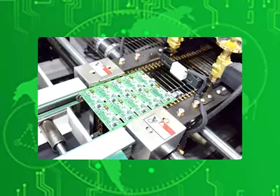
SMT basic process flow: solder paste printing -->part mounting -->reflow soldering -->AOI optical inspection -->maintenance -->board splitting
1. Solder paste printing
Solder paste is normally stored in the freezer and should be removed 12-24 hours before use to allow the solder paste to thaw independently;
The size of the steel mesh machine is 550~650mm. If the steel mesh is too small, the machine will not be able to print;
SPI: Detecting solder paste short circuits, missing prints, insufficient solder, offset, thickness, volume, and area
Each PCB must undergo self inspection, and the printed solder paste must not have any defects such as excessive or insufficient solder, continuous solder, or offset. Printed defective products should be carefully cleaned. Wipe the steel mesh promptly. Add solder paste in a timely manner to ensure the amount of solder paste rolling on the steel mesh.
2. Component mounting
SMT sequence: First attach small, low devices, then attach large, high devices
For small devices, only one chip space needs to be occupied, while large components require 2-3 chip spaces, which also affects the efficiency of the chip factory.
According to the prepared program, arrange the occupancy of components, form a material report (including material model, requirements, published occupancy, etc.), and form a sample seal as a record.
3. Reflow soldering
Reflux furnaces generally have 10 temperature zones, with better quality having 12 zones. Divided into preheating zone, constant temperature zone, welding zone, and cooling zone, the more temperature zones there are, the better the heating rate. The furnace temperature will be slightly lower than the set temperature. Maximum PCB width: 450mm.
The temperature requirements of core components need to be checked, and any requirements should be raised to the processing plant.
4. AOI optical inspection
Automatic optical online detection is used to detect the range of defects in the welded PCB board, including wrong parts, missing parts, reverse, multiple parts, reverse side, offset, insufficient tin, excessive tin, empty solder, solder beads, side standing, skewed pins, and foreign objects.
X-ray inspection: The basic principle of X-ray equipment inspection is X-ray projection microscope. Under the action of high voltage electricity, the X-ray emission tube generates X-rays that pass through the test sample (such as PCB board, SMT, etc.), and then generate images on the image receiver based on the different densities and atomic weights of the sample material itself, and the different absorption amounts of X-rays. X-RAY equipment testing is widely used in BGA testing LED、SMT、 Industries such as semiconductor and electronic machine module testing, packaging components, aluminum die castings, molded plastic parts, ceramic products, electrical and mechanical components, automation components, agriculture (seed testing) 3D printing analysis, etc. In processing plants, such as QFN packaging, the bottom of the solder pads cannot be seen and can only be viewed through X-RAY equipment.
5. Peak furnace
Wave soldering is a process technology that uses pump pressure to form a specific shape of solder wave on the surface of molten liquid solder. When the component assembly with inserted components passes through the solder wave at a certain angle, a solder joint is formed in the pin soldering area. During the process of being transported by the chain conveyor belt, the components are first preheated in the preheating area of the welding machine. In actual welding, it is usually necessary to control the preheating temperature of the component surface, so many devices have added corresponding temperature detection devices (such as infrared detectors). After preheating, the components enter the tin bath for soldering. The tin bath contains molten liquid solder, and the nozzle at the bottom of the steel bath sprays a certain shape of tin wave from the molten solder. In this way, when the solder wave passes through the component welding surface, the solder wave wets the welding area and expands and fills it, ultimately achieving the welding process.
What is EMS?
EMS stands for Electronics Manufacturing Services, which is a business model in which electronic product brands outsource manufacturing, procurement, design, and logistics to specialized vendors. Broadly speaking, it covers the entire process of product design, manufacturing, raw material procurement, logistics, testing, and after-sales service. Service providers are divided into two categories: large-scale fields (such as Hon Hai Precision, Weichuangli, etc.) and medium to small batch fields (iPCB).
The production process of EMS involves many processes and links. EMS is a comprehensive service that includes product development, production, procurement, quality management, and transportation logistics. Generally, EMS includes the above. But at the beginning, we didn't have the ability to start the entire process, so at the beginning, we mainly helped customers with the processing part, so we only managed the production part, which is called OEM (Original Equipment Manufacturer). Later on, we developed to be able to help some customers develop and design products, which is called ODM (Original Design Manufacturer). In other words, ODM has added new elements compared to OEM. Currently, EMS not only does ODM and OEM work, but also focuses on logistics and even helps customers with sales. This is the general EMS.
The main business of EMS electronic manufacturing factory covers the entire manufacturing process of electronic products. From the initial procurement of components, to product assembly, testing, packaging, and finally logistics distribution, iPCB can provide one-stop services. This service model ensures that electronic products are quickly launched into the market according to high standards and high-quality requirements.
With the rapid development of electronic information technology, the speed of electronic product updates and replacements is getting faster, and the market demand for electronic manufacturing services is also increasing. As a professional electronic manufacturing factory, EMS has advanced production technology, strict quality management system, and efficient supply chain management system, which can provide strong support for electronic product manufacturers and promote the rapid development of the electronic product industry.