A Trustworthy PCB and Electronic Manufacturing Enterprise! Contact Us


In the wave of electronic product development in 2026, transforming an excellent innovative idea into a reliable, mass-producible hardware product requires professional and efficient full-chain PCB support. As a one-stop electronic solutions provider, iPCB (iPCB Circuits Limited) is committed to offering complete services from conceptual design to finished product delivery for hardware entrepreneurs, engineers, and enterprise clients, helping you avoid common pitfalls in the development process and achieve efficient implementation of your ideas.
Every successful project starts with in-depth requirements analysis. The iPCB team conducts one-on-one communication with you to fully understand the product’s functional requirements, performance indicators, power consumption budget, size constraints, certification needs, and cost targets.
Next comes the schematic design phase. We use industry-leading EDA tools (such as Altium Designer, Cadence OrCAD, etc.) to create clear and standardized circuit schematics, ensuring logical accuracy, reasonable component selection, and early consideration of key factors like signal integrity, power distribution, and electromagnetic compatibility (EMC). This phase’s rigorous design lays a solid foundation for subsequent layout and manufacturing.
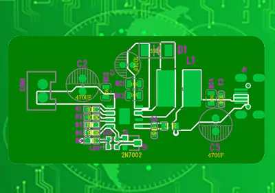
Once the schematic is confirmed correct, we move to the PCB layout phase. This is the core step in transforming abstract circuits into physical boards.
iPCB’s experienced layout engineers perform reasonable component placement, precise routing, multi-layer stack-up planning, power/ground plane segmentation, and high-frequency signal optimization based on your specific needs. We pay special attention to thermal management, signal integrity (SI/PI), and anti-interference design. For high-density or complex projects, we combine automated tools with manual expertise to ensure the layout is compact, aesthetically pleasing, and delivers excellent electrical performance.
No matter how perfect the design, if it cannot be manufactured smoothly, it amounts to nothing. iPCB places special emphasis on Design for Manufacturing (DFM), Design for Assembly (DFA), and Design for Testability (DFT) reviews.
We systematically check pad sizes, spacing, drilling accuracy, solder mask openings, silkscreen clarity, and other manufacturing specifications to avoid common issues like acid traps, shorts, or warpage. We also optimize test point distribution for easier functional testing and mass production inspection. This step significantly reduces rework rates, shortens delivery cycles, and helps clients control costs in the current supply chain environment.
After the design review passes, we quickly enter the manufacturing phase. iPCB has a mature supply chain system supporting 7-10 day rapid prototyping, with efficient production of multi-layer boards, high-frequency boards, HDI boards, rigid-flex boards, and more.
Following manufacturing, we proceed to PCBA assembly: precise SMT placement, THT insertion, reflow soldering, as well as AOI optical inspection, X-Ray inspection, and ICT/FCT functional testing to ensure every board meets high reliability standards. From prototype validation to small-batch trial production and mid-to-large-scale mass production, iPCB provides seamless full-process support to help you iterate quickly and successfully launch to market.
From creative sparks to finished hardware, iPCB’s one-stop electronic solutions accompany you through every critical step. We have successfully assisted numerous clients in realizing innovative projects in fields such as IoT devices, industrial controllers, medical electronics, and automotive electronics.
If you have an electronic product idea ready for implementation, feel free to contact sales@ipcb.com anytime for free professional consultation. The iPCB team will tailor the optimal solution for you, working together to turn your electronic ideas into reality!

Develop electronic solutions to realize your ideas