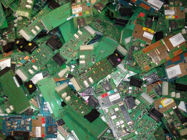
PCB sanering, or printed circuit board decontamination, is a crucial step in the modern electronic equipment recycling and processing industry. With global electronic waste (e-waste) production increasing annually, the safe and efficient disposal of used PCBs has become a pressing environmental and health issue. The core goal of this process is to completely and safely remove hazardous substances from the circuit boards while recovering valuable metals and materials, preventing them from causing irreversible harm to the environment and human health.

pcb sanering
Why is PCB Sanering Important?
The disposal of used PCBs is far more complex than recycling mobile phone cases or simple metals. The challenges stem primarily from the complexity of the materials and the integration of hazardous substances. A single circuit board is composed of over 20 different materials, including:
---Metals: copper (Cu), lead (Pb), tin (Sn), as well as high-value precious metals such as gold (Au), silver (Ag), platinum (Pt), and palladium (Pd).
---Non-metals: fiberglass epoxy resin (FR-4), solder mask, plastics, and ceramics.
---Hazardous substances: Brominated flame retardants (BFRs), lead, mercury, and cadmium.
These substances are densely packed and packed together, posing significant technical challenges for separation and recycling. Therefore, PCB sanering requires a multi-stage, high-precision processing approach.
Professional PCB Sanering Methods and Processes
The modern PCB sanering process is a highly engineered system that combines physical, thermal, and chemical treatments. It typically includes the following key steps:
1. Pre-treatment & Physical Separation
---Disassembly and Sorting: Before entering the PCB sanering processing line, manual or automated systems remove large or hazardous components, such as batteries, large capacitors, and transformers. This step prevents explosions or hazardous material leaks during subsequent processing.
---Crushing and Grinding: PCBs are fed into specialized crushers and grinders to break them down into particles as small as a few millimeters. This operation is designed to improve the efficiency of subsequent separation.
---Fine Sorting: This is the most technically demanding step. Eddy current separators are used to separate non-ferromagnetic metals (such as copper and aluminum) from non-metallic materials. Air classifiers further separate the different materials based on density and shape. Finally, electrostatic separation is used to completely separate the conductive metal from the non-conductive resin and glass fiber.
2. Pyrolysis & Thermal Treatment
---Purpose: It is a key step in PCB sanering to deal with organic matter and brominated flame retardants (BFRs).
---Technology: Pyrolysis is performed on PCB particles in an oxygen-free or low-oxygen environment. This controlled high-temperature decomposition process effectively breaks down resins and plastics and vaporizes the volatile metals. Compared to direct incineration, pyrolysis avoids the production of highly toxic dioxins and furans, a mandatory requirement for environmental regulations. The pyrolysis residue is a metal-rich carbide, providing high-quality raw material for subsequent hydrometallurgical processes.
3. Hydrometallurgy
---Purpose: To recover high-purity metals from the thermal treatment residue.
---Technology: This is a delicate chemical process. The metal-rich residue is dissolved in an acidic or alkaline solution. By precisely controlling the solution's pH, redox potential, and temperature, various pure metals can be selectively precipitated or electrolyzed. For example, base metals (such as copper and nickel) can be dissolved and recovered first, followed by the recovery of precious metals (gold and silver) using cyanide or thiourea solutions. This PCB sanering technology not only has a high recovery rate, but also can convert harmful heavy metals (such as lead and cadmium) into stable compounds, allowing safe disposal.
With the growing global emphasis on the circular economy and sustainable development, PCB sanering technology is evolving toward greater automation, lower energy consumption, and a smaller environmental footprint. As engineers, we should consider "design for recycling" during the design phase. For example, we can choose:
---Select halogen-free substrate materials to reduce the use of brominated flame retardants.
---Optimize solder formulations to minimize or eliminate the use of lead
---Simplify component packaging to facilitate automated disassembly.
Understanding and applying the principles of PCB sanering is not only about complying with environmental regulations but also about contributing to a sustainable electronics industry.