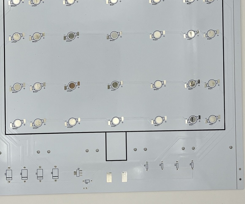
The foundation of modern electronics, from the simplest sensors to complex industrial systems, begins with the printed circuit board. Among all available configurations, the single layer PCB board remains the most fundamental and, in many cases, the most logical and economical choice.
A single-layer PCB board, also known as a single-sided board, features just one layer of conductive material (copper) laminated onto one side of an insulating substrate. Its enduring relevance in a technological landscape dominated by multi-layer complexities is rooted in its inherent simplicity, high reliability, and unparalleled cost-effectiveness. This comprehensive guide explores the structure, primary applications, and the massive economic advantages this foundational technology brings to electronic design and manufacturing.

single layer PCB board
Design Simplicity and Core Structure
The structural elegance of the single layer PCB board is its most significant asset. The board consists of four primary elements working together:
---Substrate: Typically made of FR-4 (fiberglass and epoxy resin), which provides essential mechanical strength and electrical insulation for the circuit.
---Copper Layer: A thin sheet of conductive copper foil laminated onto the substrate, where all the circuit traces, component pads, and electrical paths are etched.
---Solder Mask: A protective polymer coating applied over the copper traces to prevent oxidation, insulate against environmental factors, and prevent accidental short circuits during soldering.
---Silkscreen: The non-conductive ink layer used for printing critical information like reference designators, component outlines, and logos, facilitating easy assembly and repair.
The key benefit of this straightforward structure is realized during the layout process. Since all routing must be confined to a single plane, the design is highly predictable, straightforward, and entirely eliminates the need for complex interlayer vias or buried routing channels. This simplicity drastically reduces design time and minimizes potential errors, making the single layer PCB board the ideal solution for low-to-medium density circuits where trace crossing is minimal.
The Dominant Applications
While multi-layer configurations are essential for microprocessors and high-speed data, the single layer PCB board dominates a vast range of applications where cost, volume, and foundational simplicity are the main drivers. Its versatility makes it the default choice for numerous segments:
---High-Volume Consumer Electronics: Mass-produced items such as television remote controls, basic calculators, digital timers, and electronic toys rely heavily on this technology. The exceptionally low per-unit cost is critical for these high-volume, margin-sensitive consumer goods.
---Power Supplies and LED Lighting: Due to their robust copper layer and simple circuit paths, these boards are perfect for linear power supplies, DC-DC converters, and all forms of LED lighting systems. They efficiently handle significant current and heat with minimal circuit complexity.
---Simple Instrumentation and Control Circuits: Devices requiring basic logic and control, such as domestic appliance controls, simple sensor interfaces, relay drivers, and simple timing mechanisms, benefit from the manufacturing ease and inherent reliability of the single-layer format.
---Educational and Prototype Use: For academic labs, hobbyist projects, and rapid engineering validation where the goal is to test a circuit's functionality at the lowest possible investment, the single-sided board provides the most practical and accessible platform.
The Ultimate Cost and Manufacturing Advantage
The economic appeal of the single layer PCB board is unrivaled in the electronics manufacturing sector, offering significant benefits across the entire supply chain.
1. Cost Efficiency
The streamlined structure directly translates to the lowest possible fabrication cost. Single layer PCB boards require less raw material (only one copper foil, less prepreg), and fewer energy-intensive chemical and thermal processes (no multiple lamination cycles, no complicated through-hole plating). This minimal material use and reduced processing time drastically cut down manufacturing overhead. The resulting economic advantage makes the single-layer PCB board the essential choice for high-volume production, where even small savings per unit result in massive total cost reductions.
2. Accelerated Production and Reliability
Because the manufacturing process involves fewer steps—including a simplified drilling process that avoids the high aspect ratio challenges of multi-layer boards—the production time (lead time) is significantly faster. Furthermore, the overall manufacturing yield rate is typically higher. With fewer complex procedures, there are fewer opportunities for process-induced defects, such as layer misalignment or via plating failures. This inherently simple process ensures the final product is highly reliable and easily scalable for any size of mass production.
3. Ease of Rework and Repair
Another considerable benefit is serviceability. With all traces and component pads visible on the single surface, inspection, testing, and troubleshooting are extremely straightforward. Reworking components or repairing damaged traces is far simpler on a single-layer PCB board than attempting similar repairs on the internal, hidden layers of a complex multi-layer assembly. This ease of repair contributes to lower long-term maintenance costs over the product's lifespan.
Conclusion:
The single-layer PCB board is not an outdated technology; it is the cornerstone of efficiency in the electronics market. Its core value proposition—simple structure, reliable manufacturing, and industry-leading cost-effectiveness—makes it the definitive choice for a massive range of high-volume, cost-sensitive, and low-to-medium complexity applications. For any project where the required functionality can be achieved without the added complexity and cost of multiple routing layers, choosing the single layer PCB board offers immediate, tangible economic and reliability advantages. Partner with a manufacturer that understands how to leverage this simplicity for your next high-volume, budget-conscious product.