A Trustworthy PCB and Electronic Manufacturing Enterprise! Contact Us


In any electronic device, the power supply is the heart, pumping precisely conditioned electrical energy to every component. Without a well-designed power solution, even the most advanced processors or sensors will fail to perform reliably. The integration of power systems onto a PCB—the PCB board power supply—is a critical area of electronic design that dictates efficiency, thermal management, noise performance, and overall product longevity. Mastering the principles of power supply layout on a PCB is fundamental for all modern engineering projects.

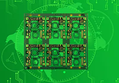
pcb board power supply
The Role of the Power Supply on a PCB
A PCB board power supply is responsible for converting an input source (like AC wall current, a battery, or a USB line) into the stable, regulated DC voltages required by the various integrated circuits (ICs) and components on the board.
Key Functional Requirements
---Voltage Regulation: Maintaining a constant output voltage despite fluctuations in the input source or changes in the load (current demand).
---Noise Suppression: Filtering out electrical noise (ripple) generated during the conversion process to ensure clean power for sensitive components (especially analog circuits).
---Efficiency: Minimizing energy loss during conversion, which directly reduces heat generation and improves battery life in portable devices.
---Protection: Incorporating features like overcurrent, overvoltage, and thermal shutdown protection to prevent damage to the board and connected systems.
Linear vs. Switching Regulators
The topology choice is the first critical step in designing a PCB board power supply. Designers typically choose between two main types of regulators: Linear and Switching.
1. Linear Regulators (LDOs)
How they work: Use a transistor in its linear region to continuously drop the input voltage down to the desired output level.
---Pros: Very low output noise (low ripple), simple to implement, and low cost.
---Cons: Low efficiency, as excess power is dissipated as heat. Suitable only for low-power applications or where noise sensitivity is paramount (e.g., radio-frequency circuits).
2. Switching Mode Power Supplies (SMPS)
How they work: Use an active switch (MOSFET) to rapidly turn the input voltage on and off, followed by an inductor and capacitor to smooth the resulting pulses into a stable DC output. Topologies include Buck (step-down), Boost (step-up), and Buck-Boost.
---Pros: High efficiency (up to 95%), making them ideal for high-power, high-current, and battery-powered applications.
---Cons: Generates significant electromagnetic interference (EMI) and ripple noise due to the high-frequency switching. Requires careful PCB layout to manage noise.
Critical PCB Layout Considerations for Power Systems
The physical layout is arguably the most challenging aspect of integrating the PCB board power supply. Poor layout can negate the advantages of the best components, leading to unstable performance and high noise.
1. A low-impedance path is essential for a stable ground reference.
---Solid Ground Planes: Using a dedicated layer (or large, contiguous pours) for the ground plane provides a low-impedance return path for current, which is essential for minimizing noise and voltage drops.
---Star Grounding: In systems combining noisy digital and sensitive analog circuits, it is best practice to separate their respective ground planes and connect them only at a single, central point (star ground). This prevents high-frequency noise from polluting the sensitive analog signals.
---Minimize Loop Area: For SMPS designs, the high-current switching paths (hot loops) must be kept as small and compact as possible. This minimizes the antenna effect, significantly reducing radiated EMI.
2. Power traces carry high current, making trace dimensions critical for two reasons:
---Current Capacity: Traces must be wide enough to safely handle the maximum current without overheating. Wider traces are mandatory for high-current rails.
---Voltage Drop: Wide traces minimize resistance, reducing the voltage drop across the path.
Designers often use copper pours (large areas of solid copper) instead of thin traces for power and ground planes to reduce impedance and aid heat spreading.
3. Decoupling and Bypass capacitors are the last line of defense against transient voltage drops and noise.
---Placement is Key: Decoupling capacitors must be placed as close as possible to the power pins of the IC they are protecting. The goal is to minimize the trace length between the capacitor and the IC pin, thus minimizing inductance and providing the fastest possible response to current demand spikes.
---Component Selection: A combination of capacitor values (e.g., a small ceramic capacitor for high-frequency noise and a larger electrolytic capacitor for bulk charge storage) is often used to ensure adequate power integrity across a wide frequency spectrum.
4. Thermal Management
Power components (especially linear regulators, switching MOSFETs, and diodes) generate heat.
---Heat Dissipation: The PCB itself is often the primary heatsink. Using thermal vias (small holes that connect copper layers) underneath heat-generating components helps quickly transfer heat away to internal or bottom copper layers for better dissipation.
---Keep Sensitive Components Away: Temperature-sensitive components, such as reference voltage ICs or precision sensors, should be placed away from hot components to maintain accuracy.
Conclusion
The successful implementation of any electronic product hinges on the reliability of its PCB board power supply. It requires more than just selecting the right regulator; it demands meticulous attention to layout design, grounding philosophy, component placement, and thermal management. By prioritizing these critical design considerations, engineers ensure that the power distributed across the board is clean, stable, and sufficient, guaranteeing the optimal performance and longevity of the entire electronic system.