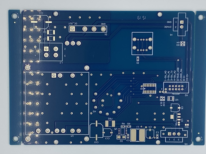
In the rapidly evolving electronics industry, the speed of product innovation determines market competitiveness. Whether it's a startup R&D company or an established electronics manufacturer, everyone knows one thing: even the most perfect design requires PCB board prototyping to verify its feasibility.

pcb board prototyping
1. The Significance of PCB Prototyping
Every electronic product relies on a fully functional, stable PCB. Before mass production, prototyping is more than just manufacturing; it serves as a systematic design verification. Through PCB board prototyping, engineers can:
---Verify circuit connectivity and signal integrity;
---Check routing and stackup stability;
---Evaluate soldering, assembly, and assembly performance;
---Simulate performance under actual use conditions.
A high-quality PCB prototype can identify potential issues early, avoiding costly rework later in the process. It also helps teams more accurately assess materials, costs, and mass production feasibility.
2. PCB Prototyping Process Overview
A standard PCB board prototyping process typically includes the following steps:
---File Preparation
The customer provides information such as Gerber files, drilling files, impedance design, and bill of materials (BOM). The completeness and accuracy of these files are crucial for the entire prototyping process.
--- Engineering Review (DFM Analysis)
Before production, engineers will conduct a Design for Manufacturability (DFM) analysis, reviewing line widths and spacing, vias, layer stackup, and solder mask spacing to ensure the design is suitable for production.
--- Material Selection and Process Determination
Based on the design requirements, select a suitable substrate, such as FR-4, Rogers, PTFE, or aluminum. Different materials have different electrical properties and heat dissipation performance, significantly impacting signal integrity and stability.
--- Manufacturing and Testing
This includes pattern transfer, drilling, plating, etching, solder mask, silk screen printing, and surface treatment. After manufacturing, the board undergoes AOI (Automated Optical Inspection), electrical testing, and visual inspection.
--- Packaging and Delivery
The finished product is typically packaged in anti-static vacuum packaging and accompanied by a test report. At this stage, the prototype board can then proceed to assembly and functional verification.
Every step of this entire process requires stringent precision and control. For high-frequency, high-speed, or multi-layer board projects, even the slightest error can result in signal distortion or functional failure.
3. The Value of PCB Prototyping
3.1 Technical Verification
Through prototype testing, designers can verify key indicators such as signal transmission quality, power distribution, and grounding performance. Prototyping is an essential step, especially in multi-layer high-speed board design.
3.2 Cost Control
Early detection of problems significantly reduces the risk of rework and scrap. Compared to design modifications during mass production, optimization during the prototype stage is less expensive and has a shorter lead time.
3.3 Process Feasibility Verification
PCB manufacturing involves not only electrical performance but also assembly, solderability, and mechanical strength. Experimental manufacturing during the prototype stage helps engineers evaluate the optimal process path.
3.4 Accelerate Time to Market
In the fiercely competitive electronics industry, those who can complete design verification and enter mass production faster are more competitive. Reliable PCB board prototyping can significantly shorten R&D cycles, enabling faster implementation of innovations.
4. Key Factors Affecting PCB Prototyping Quality
The quality of PCB board prototyping is influenced by many factors:
---Material Properties
Materials with different dielectric constants, thermal expansion coefficients, and thermal conductivity directly affect signal speed and stability. For example, high-frequency communication boards often use Rogers materials to ensure low loss and high impedance consistency.
---Process Precision
Designs such as high-density interconnects (HDI), blind and buried vias, and microvia structures place extremely high demands on process quality. Drilling, exposure, copper thickness control, and stackup positioning errors all require strict control.
---Design Matching
The degree of match between design and manufacturing determines the performance of the final product. Therefore, engineer feedback from Design for Factoring (DFM) engineers is crucial during the prototyping stage.
---Testing and Inspection Capabilities
Electrical performance testing, flying probe testing, and impedance analysis are key methods for determining whether a PCB board prototyping meets design specifications. A high-quality PCB prototyping service provider will establish standardized quality processes at every stage to ensure that prototype performance is consistent with the design.
At iPCB, we firmly believe that a high-quality PCB board prototyping can take an idea from paper to reality. With over 20 years of experience, we provide global customers with comprehensive solutions, from prototyping and sample production to small-batch trial production, ensuring the efficient implementation of every innovation.