A Trustworthy PCB and Electronic Manufacturing Enterprise! Contact Us


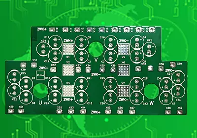

Product: High-Density TWS Bluetooth Headphone Mainboard (Integrated for wireless audio, power management, sensor control)
Material: FR-4 (Grade A, Tg 130-150°C); Deep blue UV-curable solder mask (10-12μm)
Quality standard: IPC-6012 (Class 2/3)
Dielectric constant: 4.2-4.5 @1MHz; 50Ω ±10% impedance (RF paths)
Layers: 2-4 layers (standard); 6-layer HDI (premium models)
Thickness: 0.6-0.8mm (standard); 0.55mm ultra-thin option; Tolerance ±0.05mm
Copper thickness: 1oz (35μm); 0.5oz available for fine routing
Surface technology: ENIG (120-240μ" Ni, 1-5μ" Au); Supports 0.4mm BGA, 01005 components
Special requirements: 3mil/3mil line/space; 0.2mm min aperture; EMI shielding; 280°C reflow resistance
Application: TWS headphones (audio, battery, touch, noise cancellation); portable audio devices
True Wireless Stereo (TWS) headphones rely on engineering that’s both tiny and mighty—and the TWS Headphone PCBA is that critical core. This high-density circuit board assembly is what makes crisp sound, stable Bluetooth, and all-day battery life possible in wireless earbuds. Designed for the unique demands of portable audio, it blends precision, durability, and smart design to elevate every TWS experience.
TWS Headphone PCBA
Engineered for TWS Excellence
Every aspect of this PCBA is optimized for wireless audio:
Reliable Build: Made with FR-4 (Tg 130–150°C) for stability, plus a deep blue UV-curable solder mask (10–12μm) for protection. Optional low-loss substrates support Bluetooth 5.3/LE Audio for smoother, high-quality sound .
Ultra-Dense Design: With 2–4 layers (6-layer HDI for premium noise-canceling models), it fits tiny 01005 components and 0.4mm-pitch BGAs. Fine 3mil/3mil line/space and 0.2mm min apertures let it squeeze complex tech into small earbud shells .
Connectivity & Longevity: 50Ω ±10% impedance-controlled RF paths ensure stable Bluetooth, while ENIG surface finish (120–240μ" Ni, 1–5μ" Au) resists corrosion. It handles 280°C reflow soldering for reliable assembly .
Perfect for All TWS Needs
This PCBA works across TWS categories:
Everyday Earbuds: Powers essential features—wireless audio, touch controls, battery management—with 2–4 layers and 1oz copper traces.
Premium Models: 6-layer HDI versions add advanced tech like noise cancellation, adaptive EQ, and multi-device Bluetooth pairing.
Portable Audio: Also fits in wireless speaker modules or wearable audio gadgets needing compact, efficient power.
Backed by IPC-6012 (Class 2/3), RoHS 2.0, and Bluetooth SIG compliance, the TWS Headphone PCBA is ready for mass production or custom projects. Whether you’re launching new earbuds or upgrading existing ones, the IPCB technical team can create a solution matching your audio, size, and performance goals.
Product: High-Density TWS Bluetooth Headphone Mainboard (Integrated for wireless audio, power management, sensor control)
Material: FR-4 (Grade A, Tg 130-150°C); Deep blue UV-curable solder mask (10-12μm)
Quality standard: IPC-6012 (Class 2/3)
Dielectric constant: 4.2-4.5 @1MHz; 50Ω ±10% impedance (RF paths)
Layers: 2-4 layers (standard); 6-layer HDI (premium models)
Thickness: 0.6-0.8mm (standard); 0.55mm ultra-thin option; Tolerance ±0.05mm
Copper thickness: 1oz (35μm); 0.5oz available for fine routing
Surface technology: ENIG (120-240μ" Ni, 1-5μ" Au); Supports 0.4mm BGA, 01005 components
Special requirements: 3mil/3mil line/space; 0.2mm min aperture; EMI shielding; 280°C reflow resistance
Application: TWS headphones (audio, battery, touch, noise cancellation); portable audio devices
iPCB Circuit provides support for PCB design, PCB technology, and PCBA assembly. You can request technical consultation or quotation for PCB and PCBA here, please contact email: sales@ipcb.com
We will respond very quickly.
