A Trustworthy PCB and Electronic Manufacturing Enterprise! Contact Us


RF PCB stands for radio frequency printed circuit board, which refers to high-frequency PCBs operating at frequencies above 100MHz. RF circuit board design differs from low-frequency PCB design. Due to high-frequency operation, it is more susceptible to signal integrity issues and performance degradation. For RF engineers, it is crucial to carefully consider factors such as material selection, trace layout, impedance control, and thermal management to design efficient RF boards.

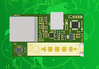
RF circuit board design
Material Selection
Common materials used in PCB manufacturing, such as FR-4, are very inexpensive but are typically not the most suitable choice for high-frequency RF applications, especially considering their uneven dielectric constants and poor tangent angles. Therefore, specific materials should be used in RF circuit board design, such as FEP, PTFE, ceramic, hydrocarbons, and various types of glass fibre. If high quality is prioritised, the best solution is to use PTFE with glass fibre; for lower costs, PTFE with a ceramic coating can be used.
Many manufacturers use Rogers materials, which are more expensive but can reduce power loss by up to 50%, ensuring high performance even above 20GHz, and featuring low dielectric constant values that remain stable and repeatable even as frequency changes. Since RF circuit boards are typically multi-layered, the most common approach is to use different materials that meet electrical performance, thermal performance, and cost requirements. For example, the outer layers can use Rogers high-performance laminates, while the inner layers can use more cost-effective epoxy glass laminates.
Stackup structure
An excellent RF PCB stackup design ensures signal and power integrity. Isolation between critical circuit modules is a key consideration in RF PCB stackup design, as it prevents interference between different RF regions and ensures separation of analogue and digital signals. Another important aspect is decoupling, which involves providing sufficient decoupling between power planes and ground planes to maintain power integrity. When designing RF circuit board stackups, it is recommended to use at least a 4-layer configuration that includes internal power planes and ground planes.
To achieve optimal RF PCB performance, it is typically recommended to use a stackup with 4 or more layers. This allows for controlled impedance routing on the outer surfaces, while the planar layers provide shielding between signal layers.
Trace layout
RF PCB traces are susceptible to transmission loss and signal interference. The primary concern in RF trace design is characteristic impedance. The most commonly used RF traces are coplanar waveguides, striplines, and microstrips.

RF circuit board design
Some best practices to follow when designing RF circuit board traces include:
-Keep RF traces as short as possible to reduce attenuation.
-Avoid placing RF traces parallel to signal traces to prevent interference.
-Test points should be placed outside the traces to maintain impedance matching values.
Thermal Management
High temperatures pose a significant challenge to RF circuit boards. This is because high temperatures alter the dielectric properties of PCB materials, thereby affecting signal propagation and phase stability. Overheating also shortens the service life of RF components, leading to premature failure and increased maintenance costs. Additionally, temperature-induced changes can cause frequency drift in RF circuits, impairing their ability to maintain precise and stable frequencies.
The following are five thermal management techniques that must be mastered in RF circuit boards design:
-Using a greater number of smaller PTHs within the ground plane can create more effective thermal paths.
-For applications where thermal conductivity is critical, use a PTH wall thickness of 0.1 mm. For standard applications, a standard 0.025 mm can be used.
-Integrate copper coins into the circuit structure. A more common method is to shape the copper coins into a stepped configuration to ensure that heat is not only effectively conducted but also evenly distributed.
-Incorporate thermal vias and thermal planes (solid copper planes) into the PCB stack to facilitate heat transfer and diffusion.
-Metal-backed circuits can effectively dissipate large amounts of heat. Examples include copper, aluminium, or brass. These circuits can be designed with pre-bonded or post-bonded structures.
In summary, RF circuit board design has extremely high requirements for materials, layering, routing, and thermal management. Selecting appropriate high-frequency materials, designing a reasonable layering structure, controlling routing impedance, and strengthening thermal management are key to ensuring signal integrity and system stability. Mastering these key points is the foundation for creating high-performance, reliable RF circuit boards.