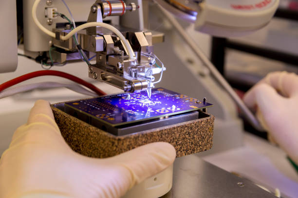
Laser is a coherent light with high energy density, strong directionality, and good monochromaticity produced by laser radiation. Its power density can reach 108 to 1080W/c㎡, and almost any metal and non-metal can be processed. Laser substrate processing refers to the irradiation of a laser beam onto the surface of the material to be processed, utilizing the energy of the laser beam to melt or remove the material as well as to change the surface properties of the material, thus achieving the processing purpose.

laser substrate
Laser substrate processing belongs to non-contact processing, with other processing technologies do not have the advantages, such as:
1. The laser cutting head will not contact the material surface, not scratching the workpiece.
2. Narrow cutting gap, saving material;
3. Small laser spot, high energy density, high precision, high speed, high stability of scribing width and depth;
4. Fine laser processing, smooth and burr-free cutting surface;
5. Small heat-affected zone, minimal local deformation of the workpiece, no mechanical deformation.
6. Good processing flexibility, can process any graphics, and can cut profiles.
Main process types of laser substrate processing technology
1. Laser drilling
Laser drilling is a highly accurate and repeatable process that can drill holes of virtually any shape and size, down to a few micrometers in diameter. In many applications, laser drilling systems can drill hundreds or thousands of holes per second.
2. Laser cutting
Laser cutting is a core technique in laser substrate processing, enabling precise and efficient material separation without physical contact. Compared to traditional cutting methods, laser cutting produces smooth, burr-free cut edges. Consistent high quality cuts are made in a wide range of materials and thicknesses. Laser cutting is driven by continuous or pulsed lasers that perforate cleanly and quickly without tool wear, while providing precise, clean cuts that result in dramatically improved sheet utilization with little or no post-processing.
3. Laser Marking
Marking is an indispensable process in the industrial production of PCBs, the purpose of which is to mark a variety of recognizable words, patterns or numbers on the surface of a product or on its outer packaging. Laser can mark a variety of textures and shapes of products, its most notable feature remains the marking of tiny objects. Many integrated circuit chips have company logos and related data printed on them, and the marking area of these chips is typically only a few millimeters to a dozen millimeters. In the past, the marking system using ink had problems such as low quality or inability to maintain permanently. After laser marking, the mark is clear and not easy to fall off.
4. Laser welding
Welding is the joining of components by heating the component boundaries so that they melt and bond. The heating process can be conveniently realized by absorbing laser light. Various laser welding processes have been developed. For seams with small or medium depths, conduction welding with medium light intensity can be used, while for deep welds with higher aspect ratios (the ratio of the depth to the width of the seam), deep welding can be used and higher light intensities can be applied. Such processes have a wide range of applications in industrial manufacturing.
Applicable Substrate Types & Materials
Laser substrate processing technology finds application in a variety of contexts, including flexible PCBs (FPCs), rigid-flex PCBs, HDI high-density interconnect boards, IC carrier boards, and ceramic substrates (Al2O3, AlN).
Due to the hard and fragile nature of the ceramic material, the through-hole preparation, shape cutting or scribing of the material is very challenging. Traditional mechanical processing methods are time-consuming and laborious, and there is a risk of damage to the substrate during processing. Laser substrate processing is a highly efficient and flexible method that offers high yield. It is characterised by its precision, speed, efficiency, large-scale batch punching, tool-free operation and other characteristics that meet the requirements of high-density interconnections in ceramic substrates. Depending on the application, blind holes, over-holes, various grooves, fine patterns or fracture lines are processed on the substrate. Should deep cavities be required, these holes can also be created using an appropriate laser process. The processing of ceramic substrates using laser technology has historically been performed using CO2 lasers. The reason for this is the fact that ceramic substrates absorb high-energy light.