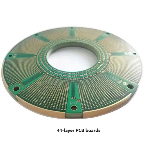
A multi-layer PCB has two or more copper layers. This is different from single-layer and double-layer PCBs, which usually have only one or two copper layers. Multilayers PCB boards usually have between 4 and 18 layers, and in special applications, they can even reach up to 100 layers. In multilayer PCB boards, the outer layers are called the top and bottom layers. The PCB has many SMD and DIP packages that allow it to do different things. In addition to the top and bottom layers, there are also multiple inner layers. These are called signal layers, power ground layers, and plane layers. These layers are connected by holes, blind holes, and buried holes to create complex electronic connections. The outer layers and inner layers are bonded together using a dielectric core and prepreg. This structure is like a sandwich, with inner layers, a dielectric core, and prepreg.

multilayer pcb boards
Features of multilayer PCB boards
Compared to single-layer or double-layer PCBs, multilayer PCB boards have several significant advantages. They are more dense, enabling more powerful functionality, greater capacity, and faster speeds. If the power and ground layers are laid out correctly, electromagnetic shielding is easier to achieve. They require less wiring, making them lighter in weight. They are smaller in size, helping to save space. They offer greater flexibility than other types of PCBs.
Multilayer PCBs are very practical, but they also have some disadvantages and limitations. The cost of multilayer PCB boards is something to consider, and you should think about the total cost of the project before choosing multilayer PCBs. It takes more time to make multilayer PCBs, so they are not a good choice for projects that need to be finished quickly. Repairing multilayer PCBs is also more complicated than repairing ordinary PCBs.
Structure and manufacture of multilayers PCB boards
Multilayer PCB boards consist of several layers of copper foils and thin laminates. These are separated by prepregs, which are glass fabrics impregnated with resin. The manufacturing process is complicated and exact, especially when blind vias (connections between an outer layer and an inner layer) or buried vias (connections exclusively between inner layers) are used. These special vias often need to be pressed multiple times to get the right layer structure. The process comprises the following steps:
—DFM Check
—Material Selection and Cutting
—Inner Layers Process
—AOI
—Lamination
—Drilling
—Copper Plating
—Outer Layer Process
—Masking and Legend Printing
—Surface Finish
—Electrical Testing
—Routing and Scoring
—Final Inspection and Packing
The future of multilayers PCB boards
The future of multilayer technology will no longer depend solely on increasing the number of layers, as this would lead to higher costs and increased risk of defects. Instead, the focus will be on optimising existing technologies and developing new materials and processes to further improve the performance, reliability and efficiency of multilayer PCB boards.
1. PCB miniaturisation and higher packaging density.
By using advanced manufacturing technologies such as laser via plating and precision etching processes, finer conductor paths and smaller vias can be achieved. This makes it possible to produce smaller, more powerful multilayer PCB boards.
2. Improving signal integrity and reducing signal loss.
By using high-frequency materials and optimised layer structures, multilayer PCBs can also be used in demanding applications such as 5G communications, high-speed data transmission, and high-frequency technology.
3. Functional integration
Integrating functions directly into PCBs is also becoming increasingly important. In addition to embedded technology (embedding components into inner layers), passive components such as resistors, capacitors, and inductors are increasingly being directly integrated into PCBs. This reduces space requirements and improves electrical performance.
4. Developing flexible and rigid-flex multilayer boards.
This combination of rigid and flexible areas enables innovative designs suitable for demanding environments such as aerospace, medical technology, or automotive electronics. Flexible multilayer PCB boards also offer advantages in terms of weight reduction and space optimisation.
5. Sustainability
This is playing an increasingly important role in the development of multilayer boards. The use of environmentally friendly materials and the introduction of recyclable printed circuit boards are key objectives in reducing the ecological footprint of the electronics industry.
Multilayer PCBs have revolutionised the electronics industry and are now an integral part of modern devices. Their ability to realise complex circuits in the smallest of spaces makes them an indispensable component of advanced technologies. With the further development of materials and manufacturing processes, multilayer PCB boards technology will continue to play a central role in electronics in the future.