A Trustworthy PCB and Electronic Manufacturing Enterprise! Contact Us



As electronic devices continue to shrink while packing higher processing power into compact enclosures, circuit board designs require increasingly fine copper traces and dense component layouts. Traditional mechanical routing or low-cost screen printing methods struggle to achieve the sub-millimeter precision demanded by modern micro-electronics. To overcome these resolution limits, hardware designers and precision manufacturers rely on photolithography—a light-driven chemical transfer process that replicates intricate circuit patterns with extreme accuracy. Utilizing a pre-sensitized photoresist PCB board allows engineers to transfer CAD-generated copper trace layouts directly onto raw laminate with micron-level fidelity, making it the ideal foundation for high-density interconnect prototyping and professional custom circuit fabrication.
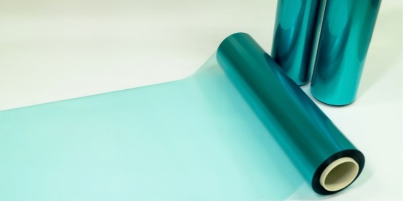
photoresist pcb board
Working Mechanism of Photoresist Coatings
The underlying magic of photolithographic circuit manufacturing relies on a photosensitive chemical polymer layer applied evenly across the copper foil of the substrate. This light-sensitive material changes its chemical solubility when exposed to ultraviolet (UV) light waves, allowing specific areas of the copper clad to be shielded during subsequent chemical etching.
Photoresist materials generally fall into two primary functional categories based on their chemical reaction during light exposure:
---Positive Photoresist: Exposure to UV radiation breaks down the polymer structure, making the exposed areas soluble in a specialized developer solution. The unexposed regions remain tough and intact, preserving the copper underneath.
---Negative Photoresist: UV light causes the active polymer molecules to cross-link and harden into a durable, chemically resistant shield. The unexposed areas remain soft and are washed away during the developing stage.In industrial board fabrication, negative resists are widely preferred due to their excellent chemical adhesion, cost-effectiveness, and strong resistance to acidic copper etching solutions. Manufacturers can apply this light-sensitive layer as a liquid wet film via roller coating or as a uniform dry film laminate applied under precise temperature and vacuum pressure.
The Step-by-Step Photolithography Process
Creating high-precision circuitry using a photoresist PCB board involves a carefully controlled sequence of chemical and mechanical processing steps to ensure pristine line edges without defects.
---Surface Preparation: The raw copper clad plate undergoes thorough mechanical scrub cleaning and chemical degreasing to remove oil, tarnish, and microscopic oxidation. A microscopically rough, clean copper surface is essential to ensure maximum resist adhesion.
---Phototool Alignment and UV Exposure: A high-contrast film artwork (phototool) containing the dark circuit trace design is placed in tight vacuum contact with the photoresist layer. The panel is then exposed to collimated UV light. The light passes through the transparent sections of the artwork while being blocked by the dark printed lines.
---Developing: The exposed board is submerged in an alkaline developer solution (such as sodium carbonate or potassium carbonate). The developer selectively dissolves the unhardened resist, revealing clean copper surfaces while leaving a tough, hardened protective mask over the intended trace pathways.
---Chemical Etching: The board travels into an acid or alkaline etching chamber (typically utilizing cupric chloride or ferric chloride). The liquid chemical solution eats away all exposed, unprotected copper foil, leaving behind the precise copper trace geometry specified in the original design files.
---Stripping: Finally, a stronger stripping solution washes away the remaining hardened photoresist film, leaving pristine, bare copper traces ready for surface finishing, solder mask application, and component assembly.
Key Advantages in Prototyping and High-Density Interconnects
Choosing a high-grade photoresist PCB board delivers immense practical benefits for projects requiring sub-millimeter trace precision and consistent electrical performance. While DIY toner-transfer methods often suffer from pitted traces, flaking toner, and bridging shorts, photoresist techniques yield crisp, smooth trace edges down to 3mil (0.075mm) line widths or thinner.
This level of photographic resolution is vital for routing fine-pitch surface-mount technology (SMT) components, such as Quad Flat Packages (QFPs) and dense Ball Grid Arrays (BGAs). Furthermore, because the light exposure process is completely non-contact, photolithography provides excellent repeatability. Engineering teams can produce identical prototype batches with zero mechanical tool wear, significantly accelerating hardware iteration cycles and reducing pre-production quality risks.
Industry Best Practices for Storage and Fabrication Quality
Achieving maximum yields when processing a photoresist PCB board demands cleanroom discipline and tight environmental parameter control throughout the manufacturing facility.
Because photoresist coatings are inherently sensitive to blue and UV spectrum light, handling and lamination processes must occur under specialized yellow safe-light conditions. Unprocessed boards must be stored in light-tight, moisture-proof packaging within temperature-controlled storage rooms to prevent premature thermal cross-linking or ambient light degradation. During the etching stage, operators must meticulously calibrate chemical solution temperature, spray pressure, and conveyor belt speed. Over-etching leads to undercutting—where the acid eats sideways under the protective photoresist mask, thinning fine traces—while under-etching leaves unwanted copper bridges between adjacent traces, causing electrical short circuits.
Conclusion
Photolithography remains the gold standard for creating high-precision copper circuit structures. Investing in an industrial-grade photoresist pcb board provides engineers with the reliable baseline needed for micron-level trace resolution and high manufacturing yields. By mastering surface prep, UV exposure, and chemical etching, your team can consistently build flawless, high-density circuit assemblies for demanding modern electronics.