A Trustworthy PCB and Electronic Manufacturing Enterprise! Contact Us



Wireless connectivity has become an indispensable feature of modern hardware engineering, driving rapid innovations across smart home automation, wearable health monitors, wireless audio systems, and industrial IoT sensors. At the core of every stable short-range wireless connection lies a specialized circuit module designed to process, amplify, and broadcast 2.4GHz radio frequency signals smoothly. Because high-frequency radio waves are extremely sensitive to spatial layout flaws, copper trace mismatches, and onboard electrical noise, building a wireless device requires far more than dropping a generic microchip onto a standard layout. Engineering a reliable bluetooth pcb board requires strict adherence to high-frequency RF layout rules, precise 50Ω impedance matching, clean power supply delivery, and robust shielding strategies to ensure uninterrupted wireless range and low latency under real-world operating conditions.
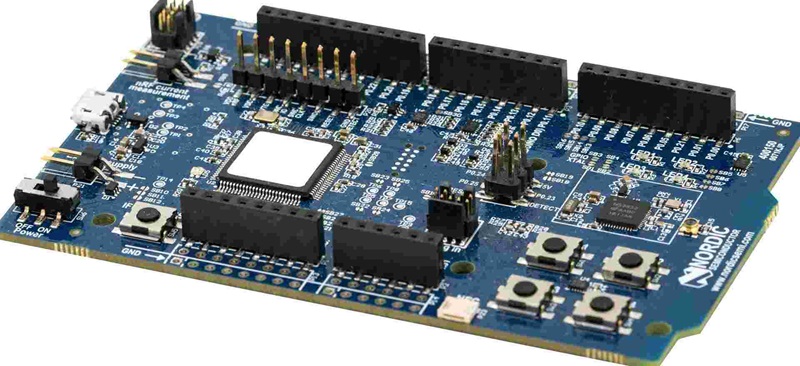
bluetooth pcb board
Antenna Design and 50Ω Impedance Matching
The antenna is the most critical component on any wireless module, serving as the bridge that converts high-frequency electrical currents inside circuit traces into electromagnetic waves travelling through free air. Designers generally choose between two primary antenna configurations depending on budget and physical space limits.
PCB trace antennas, such as the widely used Meandered Inverted-F Antenna (MIFA) or inverted-F designs, are etched directly onto the copper layer of the substrate during fabrication. They add zero component cost to the bill of materials, making them an ultra-economical choice for mass production. However, they require significant board real estate and demand a wide, clear keep-out zone completely free of underlying copper, components, or battery casings. Alternatively, surface-mount ceramic chip antennas offer an extremely compact footprint, making them perfect for miniaturized products like smart rings or fitness bands, though they require precise physical tuning during prototype assembly.
Regardless of antenna selection, maintaining an exact 50Ω characteristic impedance along the RF transmission line connecting the Bluetooth System-on-Chip (SoC) to the antenna feed point is paramount. Any sudden variation in trace width, substrate dielectric constant, or ground plane gap creates high-frequency signal reflections. These reflections bounce energy back into the transmitter, causing severe range degradation, high packet loss, and elevated battery power consumption. Layout engineers overcome this by placing a flexible Ⅱ-matching network composed of precision inductors and capacitors between the SoC output pin and the antenna, fine-tuning trace performance to eliminate impedance mismatches.
Bluetooth Low Energy and Power Management Strategy
The explosion of lightweight wearable health trackers and remote wireless sensor nodes has made energy efficiency a top priority for hardware developers. Utilizing a modern bluetooth pcb board running Bluetooth Low Energy (BLE) protocols allows hardware devices to operate continuously for months or even years on a single tiny coin-cell battery.
Achieving this extended battery life requires a carefully orchestrated power management architecture. The primary Bluetooth processor spends most of its operational life in a ultra-low-power sleep state consuming microamperes, waking up for brief milliseconds to transmit rapid bursts of data before instantly powering down again. To support these sudden transitions without crashing the system, the onboard Power Management Integrated Circuit (PMIC) or Low Dropout (LDO) regulator must supply ultra-clean voltage with minimal ripple noise. Power supply noise originating from noisy switching DC-DC converters can easily leak directly into the sensitive radio transmitter, causing carrier frequency drift and corrupted data packets.
Electromagnetic Interference Mitigation and Grounding Techniques
Operating in the globally un-licensed 2.4GHz Industrial, Scientific, and Medical (ISM) radio band means Bluetooth devices must function in a congested wireless environment filled with competing Wi-Fi routers, microwave ovens, and adjacent wireless gadgets. Furthermore, internal noise generated by onboard high-speed digital microchips, switching power lines, and LED displays can easily swamp delicate incoming wireless signals.
Mitigating interference on a complex bluetooth pcb board requires strict physical isolation between different circuit zones. Layout engineers enforce a clear structural division, isolating high-speed digital logic and power conversion components far away from the sensitive RF front-end. The area directly surrounding and beneath the RF transmission line requires a continuous, solid ground plane across internal layers to provide a short, low-impedance return path for high-frequency currents. Additionally, placing a dense wall of plated ground vias—known as via fencing—along the edges of the RF trace blocks stray electromagnetic energy from radiating into nearby analog circuits. For industrial or high-reliability applications, a stamped metal shielding can is placed directly over the central Bluetooth SoC to block external electromagnetic radiation completely.
Manufacturing Protocols and RF Testing Best Practices
Translating an optimized RF design into a high-yielding, high-performance physical product demands rigorous manufacturing controls and specialized testing procedures. Standard low-cost FR4 glass-epoxy substrates are suitable for many 2.4GHz designs, provided the fabrication facility strictly controls dielectric thickness tolerances and copper foil roughness. Variations in substrate thickness alter trace impedance, instantly degrading wireless range.
During high-speed surface mount assembly, automated pick-and-place machines must position microscopic RF capacitors and inductors with flawless accuracy, as misaligned components or excess solder paste introduce parasitic capacitance that detunes the antenna network. Before shipping completed units to customers, every assembled bluetooth pcb board must pass rigorous end-of-line RF testing. Automated production test stations utilize Vector Network Analyzers (VNAs) and specialized RF testing fixtures to measure real-world parameters, including return loss (S11), carrier output power, receiver sensitivity, and harmonic emissions to guarantee full compliance with global regulatory standards like FCC and CE.
Conclusion
Creating a reliable short-range wireless product demands an uncompromising focus on high-frequency RF engineering principles from the very beginning of the layout process. Treating wireless connectivity as an afterthought or neglecting strict layout rules inevitably leads to dropped connections, reduced range, rapid battery drain, and failed regulatory certifications out in the field. Partnering with an experienced electronics manufacturing facility that understands the strict tolerances required for a custom bluetooth pcb board ensures that your wireless design transitions smoothly from theoretical schematic files into a ruggedized, high-yielding physical product. By optimizing 50Ω trace geometry, maintaining clean power delivery networks, implementing robust ground planes, and enforcing comprehensive RF production testing, your engineering team can deliver high-performance wireless products that keep users seamlessly connected everywhere.