A Trustworthy PCB and Electronic Manufacturing Enterprise! Contact Us


In the current landscape of digital innovation, the boundary between "standard" and "high-speed" electronics has largely disappeared. Whether you are designing for AI computing, 5G communications, or high-definition video processing, the speed of signal rise and fall times dictates the complexity of your board. Unlike low-speed designs, where connectivity is the primary goal, a successful high speed PCB layout requires treating every trace as a transmission line. At these frequencies, the physical geometry of the copper, the properties of the dielectric, and even the proximity of the housing can cause reflections, crosstalk, and timing errors. Mastering the delicate balance of electromagnetics and physical constraints is essential for ensuring your hardware performs reliably under high-speed data loads.

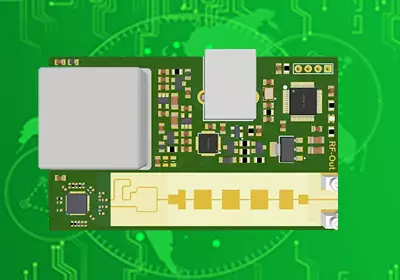
high speed pcb
The Core of High Speed Performance – Layer Stack-up
The foundation of any high-speed system is its layer stack-up. In a high speed PCB layout, the goal is to provide a clear, low-impedance return path for every signal. This is achieved by placing a solid ground plane (GND) directly adjacent to every signal layer. This configuration minimizes the "loop area," which in turn reduces electromagnetic radiation and susceptibility to noise.
Furthermore, engineers must consider the "Skin Effect," where high-frequency signals travel only on the outer surface of the conductor. By selecting high-performance materials like Rogers or Isola with low dielectric loss (Df), manufacturers can ensure that signal attenuation remains manageable even over long trace lengths. A well-planned stack-up is the most cost-effective insurance policy against EMI failures during compliance testing.
Precision Trace Routing and Impedance Control
In high-speed design, the physical shape of the trace determines its electrical behavior. To prevent signal reflections, the characteristic impedance (typically 50Ω single-ended or 100Ω differential) must remain constant from the driver to the receiver.
When executing a high speed PCB layout, designers must pay close attention to "discontinuities." A common mistake is using sharp 90-degree bends, which cause a sudden change in trace width and impedance. Instead, 45-degree angles or smooth curves are used to maintain uniformity. Differential pairs—used for protocols like PCIe and USB 4.0—require strict length matching. Even a tiny mismatch in length can cause a phase shift, turning a clean digital signal into a noisy mess of common-mode interference.
Mitigating Crosstalk and Electromagnetic Interference
Crosstalk occurs when the electromagnetic field from one trace "bleeds" into an adjacent one. In a dense high speed PCB layout, managing this interference is critical. The "3W Rule" is a standard guideline, stating that the spacing between traces should be at least three times the width of the trace itself to minimize coupling.
For highly sensitive signals, such as system clocks or high-speed transceivers, designers often use "GND Guarding"—placing ground copper around the trace to act as a shield. Additionally, vias (the vertical interconnections between layers) should be used sparingly. Each via adds parasitic capacitance and inductance; if a via is necessary, "stitching vias" should be placed nearby to ensure the return path follows the signal through the board layers without interruption.
Decoupling and Power Integrity Strategies
Signal integrity cannot exist without power integrity. A high-speed chip can draw significant bursts of current in nanoseconds, which can cause "ground bounce" or voltage sags if the power distribution network (PDN) is weak. The strategy involves placing decoupling capacitors as close as possible to the power pins of the IC.
These capacitors act as local energy reservoirs, smoothing out voltage ripples before they can affect the signal. In advanced layouts, multiple capacitors of varying values (0.1\muF, 0.01\muF, etc.) are used to filter noise across a wide frequency spectrum. Using solid power planes instead of thin traces further reduces the PDN impedance, ensuring the silicon receives the stable, clean energy it needs to function at maximum clock speeds.
Conclusion
Precision and discipline are the hallmarks of a world-class hardware engineer. As we move toward 6G and increasingly complex autonomous systems, the challenges of electromagnetic field management will only intensify. A professional high speed PCB layout is not just about connecting pins; it is about creating a controlled environment where electrons can travel at gigahertz speeds without interference. By mastering stack-up design, impedance control, and power integrity, you can transform a theoretical circuit into a robust, high-performance reality. In the competitive race for bandwidth and speed, the integrity of your layout is what will define the performance limits of your next-generation innovation.