A Trustworthy PCB and Electronic Manufacturing Enterprise! Contact Us


Every groundbreaking electronic product, from a smart kitchen appliance to a massive robotics system, begins its journey as a messy tangle of jumper wires on a prototype breadboard. While breadboards are excellent for validating a proof of concept, they are notoriously unreliable for long-term testing due to loose mechanical connections and stray capacitance. Moving your circuit onto a dedicated green substrate is the ultimate way to secure your hardware footprint. Engaging in a simple PCB board design allows developers to transform unstable, loose components into a single, rugged, professional-grade module. However, even when a circuit involves only a few dozen components, bypassing standard manufacturing rules can lead to alignment failures or electrical shorts, making a systematic approach to layout and fabrication essential.

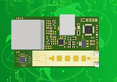
simple pcb board design
Translating Ideas into a Clean Schematic Diagram
The absolute foundation of any electronics layout is the schematic diagram. Think of the schematic as the blueprint of your house; it defines exactly which electrical connections exist without worrying about where the components physically sit on the board.
During this initial phase, engineers select the electronic footprints for basic parts like resistors, capacitors, microcontrollers, and power terminals. A common trap in basic engineering is drawing chaotic wires that cross over one another, which leads to confusion during the layout stage. Using net labels—naming specific connection nodes such as VCC, GND, or TX—keeps the document clean and easy to read. A perfectly organized schematic guarantees that the automated software netlist will transfer to the next physical stage without missing a single crucial electrical connection.
Layout Placement Strategy for Two-Layer Architectures
Once the schematic is fully verified, the workflow shifts to the physical board layout window. When executing a simple PCB board design, a standard two-layer FR4 stack-up is typically the most economical and efficient choice. Component placement is the most critical stage of this process, as poor placement makes subsequent trace routing almost impossible.
A professional layout practice is to follow a logical signal flow, positioning components from input to output. For instance, voltage regulators and input power terminals should sit near the board periphery, while the main processor takes center stage, and decoupling capacitors sit immediately next to the IC power pins. Grouping related analog or digital components prevents crosstalk and keeps trace lengths as short as possible. Additionally, placing all heavy connectors along the edges of the board ensures that external cables do not strain delicate internal components during daily operation.
Routing Basics and Power Integrity Rules
With all components locked into their optimal positions, the process of drawing the actual copper paths, known as routing, begins. For an effective, simple PCB board design, trace width is the primary parameter that governs electrical performance. While a thin 0.2 mm (8 mils) trace is perfectly adequate for low-power communication signals like UART or I2C, power rails require much wider tracks to carry current safely without heating up.
Furthermore, designers must implement a solid ground pour on the bottom copper layer. Instead of running individual thin traces for every ground connection, filling the empty areas of the substrate with a continuous sheet of copper ground plane provides an immediate, low-impedance shield. This ground plane acts as a return path for all high-frequency currents, significantly cutting down on electromagnetic noise and protecting sensitive analog circuitry from external interference.
Preparing Design Files for Error-Free Manufacturing
The final bridge between software layout and physical manufacturing is running a rigorous Design Rule Check (DRC). Even an experienced engineer can occasionally run a trace too close to a mechanical mounting hole or accidentally bridge two pads. The DRC tool evaluates your completed simple PCB board design against the specific manufacturing tolerances of your fabrication house, automatically flagging errors like insufficient trace spacing or narrow annular rings before the files go to production.
Once the DRC passes with zero errors, you export the industry-standard Gerber files and Excellon drill files. These packages act as the universal language for computerized milling and plating machinery. Providing an accurate Bill of Materials (BOM) alongside your Gerber data ensures that the factory assembly line can identify and solder every component perfectly, leading to a high-yield production run on your very first try.
Conclusion
Mastering the baseline mechanics of hardware layout is an invaluable skill that unlocks infinite opportunities for tech innovation. Whether you are building a bespoke testing rig for an industrial laboratory or launching a consumer hardware startup, starting with a disciplined approach to trace widths, ground plane placement, and manufacturing guidelines saves months of debugging time. A well-executed simple PCB board design provides the perfect balance between low fabrication costs and long-term hardware reliability, turning a basic concept into a robust asset. By establishing clean design rules early in your engineering cycle, you guarantee a smooth manufacturing process and create a solid foundation for more complex multilayer projects in the future.