A Trustworthy PCB and Electronic Manufacturing Enterprise! Contact Us



When electronic hobbyists, students, and professional hardware designers graduate from basic single-layer layouts, they quickly encounter projects that require crossing electrical traces without creating short circuits. While single-sided circuit boards limit trace routing to a single flat plane, modern electronic circuits demand much higher connection density and signal flexibility. To bridge this engineering gap, hardware engineers rely on a versatile double sided copper clad PCB board, which features conductive copper foil laminated onto both the top and bottom surfaces of the insulating substrate. This dual-layer architecture unlocks advanced circuit routing, improved power distribution, and compact device designs across countless consumer and industrial electronics.
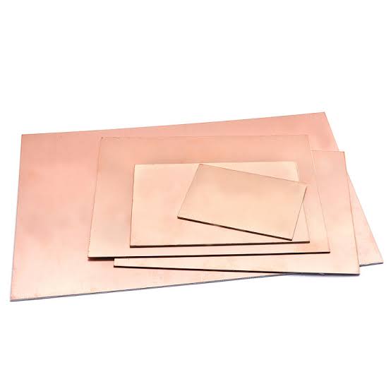
double sided copper clad pcb board
Core Physical Structure and Layer Anatomy
To appreciate how a dual-layer circuit operates, it helps to examine its fundamental physical composition. A standard commercial laminate consists of a rigid central core made of woven fiberglass and epoxy resin, known globally as FR4.
Unlike single-sided laminates, a double sided copper clad PCB board sandwiches this insulating fiberglass core between two thin, highly conductive layers of rolled-annealed or electrolytic copper foil. These top and bottom copper sheets act as separate metallic highways for electrical signals. However, copper layers on opposite sides of the board cannot talk to each other unless an electrical bridge connects them through the fiberglass. This vital connection is achieved through plated through-holes (PTH)—tiny, copper-coated cylindrical barrels drilled directly through the board that allow current and data signals to travel seamlessly between the top and bottom layers.
Design Rules and Routing Strategies for Makers
Designing a circuit layout for a double sided copper clad PCB board requires a strategic shift in thinking compared to single-layer layouts. Instead of squeezing every single trace onto one crowded surface, layout engineers can split signals logically between the top and bottom layers.
A common industry standard is orthogonal routing: running all primary signal traces horizontally on the top copper layer, while running vertical traces and power distribution lines on the bottom layer. This grid-like approach prevents parallel traces from running directly on top of each other, drastically reducing electromagnetic crosstalk. Furthermore, filling unused open areas on both layers with solid copper pours connected to ground (GND) creates a low-impedance ground reference plane that shields sensitive signals from external electrical noise.
Industrial Etching and Plated-Through-Hole Manufacturing
Transforming a blank piece of raw material into a finished, multi-layered electronic substrate involves advanced chemical and mechanical processing inside industrial cleanrooms. Fabricating a professional double sided copper clad PCB board begins with precise photolithography, where ultraviolet light transfers circuit patterns onto light-sensitive photoresist coatings applied over the copper.
Once the unwanted copper areas are chemically etched away in acid baths, the panel undergoes precision mechanical drilling to create component holes. Because raw fiberglass is non-conductive, bare drilled holes must undergo electroless copper deposition—a complex chemical plating bath that deposits a microscopic layer of pure copper onto the rough internal walls of every hole. Subsequent electroplating thickens this barrel copper, ensuring that when components are soldered later, electrical continuity between the top and bottom layers remains 100% reliable.
Hand Soldering and Component Assembly Best Practices
Assembling electronic components onto a dual-layer substrate on your workshop bench requires careful soldering discipline. Because both sides feature exposed copper pads and plated holes, heat management is critical to prevent lifting delicate copper pads off the fiberglass substrate.
When populating a double sided copper clad PCB board, always install low-profile components (such as surface-mount resistors, diodes, and IC sockets) first, before moving on to taller parts like electrolytic capacitors and heavy power connectors. When soldering through-hole component leads that pass all the way through to the top layer, apply your soldering iron tip to both the lead and the bottom pad simultaneously, feeding just enough solder to fill the barrel completely. On double-sided boards without plated through-holes (such as basic DIY copper-clad boards), you must manually insert a short wire jumper through the hole and solder both sides to ensure the top and bottom circuits connect properly.
Conclusion
Dual-layer printed circuit technology represents the foundation of modern electronic engineering, offering the perfect balance between manufacturing cost, design flexibility, and signal routing complexity. Whether you are designing an IoT sensor module, an audio amplifier, or a custom microcontroller development kit, mastering dual-layer layouts is an essential milestone. Utilizing a high-quality double sided copper clad PCB board empowers engineers and makers to route complex schematics, control electromagnetic interference, and build durable hardware products ready for the modern technological landscape. By combining smart layer partitioning with clean hand-soldering techniques, you can successfully turn advanced electronic concepts into reliable working realities.