A Trustworthy PCB and Electronic Manufacturing Enterprise! Contact Us



Modern computing systems demand unprecedented levels of processing power, rapid data transfer rates, and flawless multitasking capabilities. Whether powering cloud data center servers, artificial intelligence accelerators, high-end gaming rigs, or compact laptops, the hardware foundation remains identical. Every processor, memory stick, voltage regulator, and high-speed storage drive relies on a central nervous system to exchange billions of signals every second without error. Engineering a high-performance computer circuit board requires a deep masterclass in advanced multilayer stackup architecture, precise high-speed signal routing, robust thermal dissipation, and rigorous quality inspection standards to ensure absolute processing stability under heavy computational workloads.
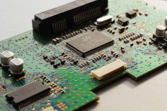
computer circuit board
Multilayer Architecture and High Density Interconnect Technology
Modern computer architectures integrate thousands of microscopic connection pins into ultra-dense Integrated Circuit (IC) packages like CPUs, GPUs, and chipsets. Routing these thousands of individual electrical connections cleanly across a physical panel requires shifting from simple double-sided boards to complex multilayer stackups, often ranging from 8 to more than 20 distinct copper layers.
To accommodate this extreme routing density within compact form factors, electronics engineers utilize High-Density Interconnect (HDI) technology. HDI designs employ laser-drilled microvias, blind vias (which connect surface layers to internal layers), and buried vias (which connect internal layers only). These micro-structures allow components with tiny pin pitches, such as Ball Grid Arrays (BGAs), to break out signals efficiently. By replacing traditional through-hole vias with microvias, layout designers free up critical internal copper space, shorten signal path lengths, and drastically increase trace routing density across the entire substrate.
High Speed Signal Integrity and Impedance Control
As data transmission standards evolve into ultra-fast domains like PCIe 5.0, PCIe 6.0, and DDR5 memory channels, maintaining crisp signal integrity across a computer circuit board becomes an intense physical challenge. At multi-gigahertz operational frequencies, standard copper traces stop behaving like simple electrical wires and start acting like complex transmission lines subject to high-frequency wave physics.
Layout engineers must enforce strict controlled impedance rules across the entire layout. Differential trace pairs used in high-speed data buses must maintain continuous, precise spacing and trace widths to achieve target single-ended (50Ω) or differential (100Ω) characteristic impedance. Any sudden disruption in trace geometry, layer transitions, or ground reference gaps causes immediate high-frequency signal reflections, wave distortion, and bit errors. Furthermore, placing solid, uninterrupted ground reference planes adjacent to high-speed signal layers blocks electromagnetic crosstalk between parallel traces, ensuring clean data transmission across computing buses.
Power Delivery Network and Thermal Management
High-performance computational processors draw immense electrical current, often exceeding 100 to 200 amperes at extremely low supply voltages (1.0V or below). Delivering this massive, stable current from the Power Management IC (PMIC) or Voltage Regulator Modules (VRMs) directly to the CPU silicon die requires a meticulously engineered Power Delivery Network (PDN).
A well-designed computer circuit board incorporates thick copper power planes (2 oz or higher) and dense arrays of low-ESR ceramic decoupling capacitors placed directly beneath the processor socket. These capacitors store local energy reserves to smooth out rapid current spikes caused by heavy processing tasks, preventing logic errors caused by voltage droops. Additionally, because high-power computing components generate significant heat, boards integrate dense thermal via arrays beneath hot power MOSFETs and employ high-Tg (glass transition temperature) laminate materials to dissipate heat efficiently across internal copper layers without substrate warping.
Advanced Manufacturing Protocols and Reliability Testing
Translating a complex multi-gigahertz computing architecture from computer-aided design (CAD) software into a physical product requires ultra-precise factory manufacturing standards. Fabrication plants select specialized low-loss FR4 or high-frequency laminate materials featuring low dielectric constants (Dk) and minimal loss tangents (Df) to minimize high-frequency signal attenuation over long traces.
During automated Surface Mount Technology (SMT) assembly, high-precision pick-and-place systems position micro-components onto solder paste with sub-millimeter accuracy. Once reflow soldering is complete, every manufactured computer circuit board passes through rigorous multi-stage quality testing. Automated Optical Inspection (AOI) checks component orientation and solder joint quality, while X-Ray Inspection penetrates deep beneath BGA chips to verify hidden solder ball formation and detect microscopic solder bridges. Finally, in-circuit electrical testing validates continuity and impedance parameters before final chassis integration.
Conclusion
Building modern digital hardware requires combining high-speed electronics theory with precise manufacturing execution. From managing multi-layer HDI stackups and 50Ω impedance lines to building low-noise power delivery networks, every design decision impacts overall processing speed, heat output, and long-term hardware reliability. Partnering with a dedicated PCB manufacturing facility that understands high-density routing and strict high-frequency testing rules ensures that your custom computer circuit board delivers smooth, uninterrupted processing performance across years of intense operation. By prioritizing clean layout engineering and rigorous quality verification, your engineering team can build resilient hardware platforms ready to power the future of computing.