A Trustworthy PCB and Electronic Manufacturing Enterprise! Contact Us



Every modern electronic device, from high-performance cloud servers and industrial robotics to medical equipment and consumer electronics, relies on a continuous delivery of clean, stable electrical energy. Converting high-voltage AC mains power or fluctuating battery DC inputs into precise, noise-free voltages requires sophisticated power management architecture. Because high-current switching conversion inherently generates thermal stress, high voltage potential, and electromagnetic noise, standard layout practices are insufficient for power systems. Designing a rugged power supply PCB board demands meticulous attention to trace current capacity, thermal dissipation paths, grounding isolation, and safety clearance rules to guarantee long-term operational reliability and prevent catastrophic component failures out in the field.
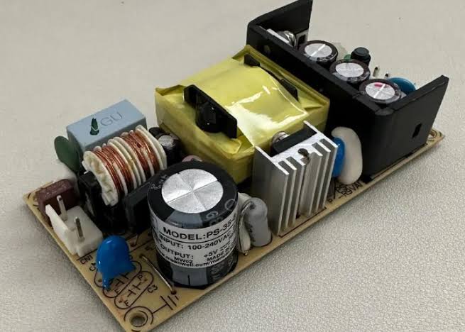
power supply pcb board
Trace Width and Heavy Copper Design for High Current Handling
The primary task of any power distribution network is delivering substantial electrical currents without causing excessive voltage drops or overheating the circuit traces. Standard circuit boards typically utilize 1oz/ft2 (35 µm) copper foil, which is suitable for microamps of digital signals but rapidly overheats under heavy power loads.
To handle tens or hundreds of amperes safely, designers must carefully calculate copper trace widths based on IPC-2152 thermal standards. When space limitations prevent laying down ultra-wide surface traces, incorporating heavy copper substrates featuring 2oz to 6oz (or higher) copper thickness becomes essential. Increasing copper thickness reduces internal resistive I2R power losses, keeps temperature rise within safe operational limits, and lowers overall board temperatures without expanding the physical footprint of the unit.
Thermal Management Strategies and Heat Dissipation
Active power conversion components, such as switching MOSFETs, Schottky diodes, and power inductors, inevitably convert a portion of electrical energy into wasted heat during operation. Accumulating unhandled heat degrades silicon junction lifespans and can trigger premature thermal shutdown in a power supply PCB board.
Hardware engineers utilize multiple complementary heat dissipation techniques to manage these thermal loads effectively:
---Thermal Via Arrays: Placing dense matrices of copper-plated through-holes directly beneath hot surface-mount power packages transfers thermal energy efficiently down to internal or bottom-layer ground copper planes.
---Metal Core Substrates: For extreme power density applications, such as LED drivers or automotive power units, using Aluminum or Copper Metal Core PCBs (MCPCB) dramatically boosts thermal conductivity compared to standard FR4 glass-epoxy laminates.
---Dedicated Heatsinks and Airflow Paths: Mounting heavy extruded aluminum heatsinks directly onto power semiconductors while aligning major heat-generating components along forced air paths ensures continuous convection cooling.
Electromagnetic Interference Mitigation and Grounding Layout
Switching Mode Power Supplies (SMPS) offer high energy efficiency, but their rapid voltage and current switching transitions (dV/dt and dI/dt) generate substantial high-frequency electromagnetic interference (EMI). Uncontrolled noise can easily pollute nearby sensitive analog sensor lines or fail international regulatory compliance limits.
Designing a low-noise power supply PCB board requires keeping high-frequency AC current loops as physically compact as possible. Reducing the physical area of the primary switching loop formed by the input capacitor, switching transistor, and freewheeling diode minimizes magnetic field radiation. Furthermore, engineers must strictly separate high-current power ground planes from delicate control signal ground traces. Connecting these distinct ground planes at a single designated star-ground point prevents noisy switching return currents from corrupting sensitive voltage feedback loops.
Safety Clearances and Manufacturing Quality Standards
When converting high-voltage AC inputs to low-voltage DC outputs, maintaining physical electrical isolation is mandatory to protect end-users from lethal electric shocks and prevent short-circuit arc-overs.
Layout engineers must follow strict IPC-2221 guidelines regarding clearance (the shortest distance through air between two conductive traces) and creepage (the shortest distance along the surface of the insulating substrate). In high-humidity or contaminated environments, mill-cut isolation slots or protective conformal coatings are applied along high-voltage boundaries to prevent electrical tracking across the substrate surface. During manufacturing, every assembled power supply PCB board undergoes mandatory High-Potential (Hi-Pot) insulation testing, automated optical inspection (AOI), and infrared thermal imaging under full operational load to verify structural integrity before final enclosure integration.
Conclusion
Power delivery systems serve as the foundation of modern hardware systems, where component failure or thermal stress can compromise an entire system. Achieving excellent voltage regulation, low electromagnetic noise, and cool operational temperatures requires deep expertise across high-current copper sizing, thermal via placement, noise-reducing grounding strategies, and high-voltage safety clearances. Partnering with a specialized manufacturing plant capable of processing heavy copper foils and enforcing strict insulation testing ensures that your custom power supply PCB board delivers uninterrupted, high-efficiency power across years of demanding field operations. By combining robust schematic engineering with rigorous manufacturing protocols, your team can deploy dependable hardware platforms ready to meet the toughest energy challenges.