A Trustworthy PCB and Electronic Manufacturing Enterprise! Contact Us



Every modern electronic product, from high-end smartphones and industrial automation controllers to smart home appliances and automotive infotainment displays, relies on a central physical system to route power, process data, and coordinate hardware tasks. This primary computing platform acts as the true structural backbone and operational brain of the entire hardware ecosystem. Because it hosts the most critical microprocessors, wireless communication modules, and power conversion circuits, any flaw in its architectural layout can severely throttle performance or cause sudden system crashes. Designing a high-reliability main PCB board requires a thorough balance between high-density signal routing, advanced thermal dissipation, and ironclad manufacturing standards to ensure seamless performance under rigorous daily usage.
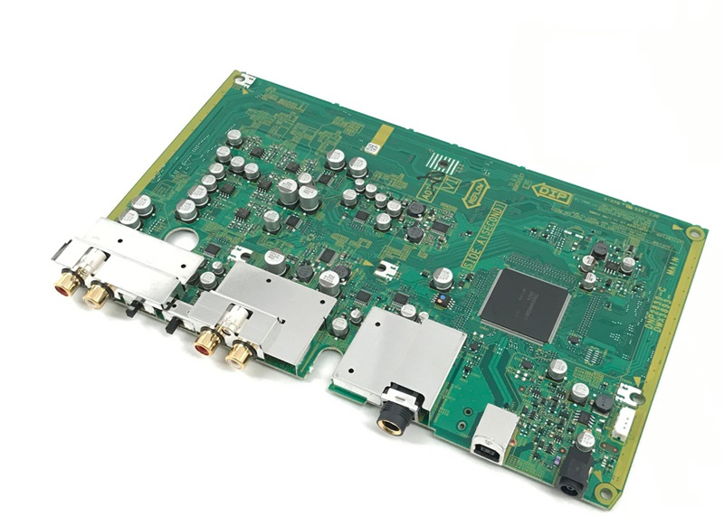
main pcb board
Architecture and Subsystem Integration
The architectural complexity of a primary circuit board lies in its ability to consolidate wildly different electrical sub-systems into a single, compact footprint. A typical high-performance platform must accommodate powerful multi-core central processing units, high-speed RAM chips, power management integrated circuits (PMICs), and sensitive radio frequency (RF) antennas without allowing these components to interfere with one another.
To achieve harmony across these subsystems, hardware engineers divide the board space into logical functional zones. High-power switching circuits are isolated far from delicate analog audio or sensor inputs, preventing power noise from corrupting low-voltage telemetry. Meanwhile, high-speed memory buses are kept extremely short and direct, minimizing trace length variations to ensure that billions of data clock cycles arrive at their destination at precisely the exact microsecond without timing drift.
Multi-Layer Stackup and Impedance Control
As device footprints continue to shrink while computing demands skyrocket, routing all required signal pathways on simple two-layer or four-layer substrates has become virtually impossible. Modern high-speed designs frequently demand complex 6-layer to 12-layer stackups featuring dedicated internal ground and power reference planes. Specifying a premium main PCB board stackup ensures that every sensitive high-speed signal trace is sandwiched cleanly between continuous reference planes, forming low-EMI microstrip and stripline structures.
A cornerstone of high-speed digital engineering is strict impedance control. When data signals travel through circuit traces at gigahertz frequencies, any sudden mismatch in trace width, copper thickness, or distance to the ground plane causes signal reflections that corrupt data packets. Fabrication plants utilize specialized high-frequency laminates and precise laser-etching techniques to maintain uniform trace impedance tolerances within five percent, guaranteeing crisp signal integrity across every data lane.
Thermal Management and Power Distribution Strategy
With ultra-fast processors running complex operating systems, managing localized heat accumulation is vital to preventing thermal throttling and thermal degradation. High-performance central processing units and onboard voltage regulator modules (VRMs) generate intense heat during heavy computing tasks. If this thermal energy remains trapped underneath active silicon dies, component temperatures will rise rapidly, reducing power efficiency and causing physical warping over extended service periods.
Optimizing a main PCB board layout involves turning the copper planes themselves into massive passive heat sinks. Engineers integrate wide, heavy copper power pours across internal layers and place dense matrices of plated thermal vias directly under high-heat microchips. These copper thermal expressways pull heat downwards away from the top components, spreading it uniformly across the entire board surface where it can dissipate into the surrounding chassis air or through attached thermal pads and metal shielding cans.
Manufacturing Quality Control and Testing Protocols
Translating a dense multi-layer Gerber design into a flawless physical product requires high-precision manufacturing processes and multi-stage automated testing. Because modern microprocessors feature tiny Ball Grid Array (BGA) packages with hundreds of microscopic solder balls tucked underneath the chip body, traditional visual inspection methods are completely inadequate for detecting modern assembly faults.
Professional assembly plants utilize High-Definition Automated Optical Inspection (AOI) to verify surface component placement and high-power 3D X-ray systems to inspect hidden solder joints under BGA packages. After the physical soldering stage is complete, every completed main PCB board undergoes comprehensive testing routines. Bed-of-nails In-Circuit Testing (ICT) verifies trace continuity and component values, while rigorous Functional Testing (FCT) powers up the board to execute full software boot sequences, ensuring that every interface port and processing core functions perfectly before final product integration.
Conclusion
Developing a durable, high-performance computing platform requires equal mastery over micro-electronic architecture, high-speed signal integrity, thermal management, and strict quality assurance protocols. While consumer choices are often driven by exterior product aesthetics and sleek casing designs, true long-term product success is dictated entirely by the stability of the inner processing engine. Investing the necessary engineering resources to optimize trace routing, refine thermal via placement, enforce precise impedance targets, and partner with a certified fabrication facility guarantees that your main PCB board delivers exceptional computing speed and unbroken hardware reliability. By treating the central circuit assembly as the foundational pillar of your product ecosystem, your engineering team can eliminate unexpected field failures, extend device operating lifetimes, and establish an enviable reputation for quality in the competitive global tech market.