A Trustworthy PCB and Electronic Manufacturing Enterprise! Contact Us


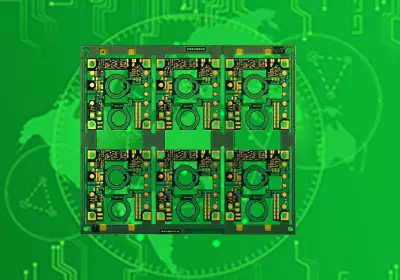
Every great electronic hardware invention begins with a simple idea, a hand-drawn schematic, and a spark of curiosity. However, bridging the gap between a digital computer simulation and a physical, working device requires a hands-on testing phase. While temporary plug-in breadboards are fantastic for quickly checking basic logic, they are notoriously fragile and prone to loose connections when bumped or moved. When electronic makers and professional hardware engineers need to lock down their schematic designs into a semi-permanent, reliable physical format, they turn to a high-quality proto board PCB. This versatile prototyping platform allows you to solder components securely into place, transforming loose components into a rugged, functional hardware prototype ready for rigorous real-world testing.
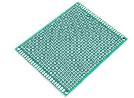
proto board pcb
Exploring Perfboards and Stripboards
Before diving into hardware assembly, it helps to understand the different physical styles available on the market. Prototype boards generally fall into two main categories based on how their copper pads are interconnected underneath the surface.
The first style is the standard perfboard, where every single through-hole features an isolated copper ring on one or both sides. This layout gives the designer complete freedom to place components anywhere and route connections manually using insulated hook-up wire or solder bridges. The second style is the stripboard, which features parallel rows of copper tracks running across the entire length of the board. Stripboards save significant wiring time for linear circuits, though designers must sometimes scrape away small sections of copper to break paths and prevent unwanted electrical short circuits between adjacent component pins.
Benefits of Using a Proto Board PCB for Circuit Testing
Transitioning your project from a loose plastic breadboard onto a soldered proto board PCB unlocks immediate performance and durability benefits. On a standard breadboard, spring clips can oxidize over time, introducing high electrical resistance and intermittent signal dropouts that frustrate debugging sessions.
Soldering components directly onto a rigid fiberglass substrate eliminates loose connections instantly. The solid copper pads provide low-resistance electrical pathways and strong mechanical support for heavy components like toggle switches, screw terminals, and power regulators. Furthermore, fixing your layout onto a permanent substrate significantly reduces stray capacitance and parasitic inductance compared to messy jumper wire nests, ensuring your microcontroller or analog sensor circuit operates with stable electrical performance during initial laboratory bench testing.
Best Practices for Layout and Soldering on a Proto Board PCB
Building a clean, professional circuit on a proto board PCB requires patience, logical component placement, and disciplined soldering technique. Unlike automated factory circuit boards, you are acting as the manual layout routing engine, so planning ahead prevents frustrating wiring mistakes.
Start by placing large components—such as electrolytic capacitors, connectors, and integrated circuit sockets—on the top side of the board before flipping it over to route your connections. Group your circuit into logical functional zones, keeping noisy switching power regulators far away from sensitive analog sensor inputs. When soldering, use clean resin-core solder and a temperature-controlled iron set around 350℃. Apply heat evenly to both the component lead and the copper pad simultaneously for two to three seconds, feeding just enough solder to form a shiny, concave, volcano-shaped joint without creating accidental bridges between adjacent holes.
Moving From Prototype to Professional Production
The ultimate goal of building an initial circuit proof-of-concept is validating that your schematic design actually functions as intended in the physical world. Once your hand-wired prototype is fully debugged and operational, the next natural step in the product development lifecycle is transitioning toward custom automated manufacturing.
Documenting every connection on your working proto board PCB allows you to recreate the schematic accurately in professional Electronic Design Automation (EDA) software like KiCad or Altium Designer. From there, you can route clean digital copper traces, generate standard Gerber manufacturing files, and order custom double-sided or multi-layer printed circuit boards from an industrial fabrication plant. This evolution from a handmade workshop experiment to a polished, mass-produced product represents the core journey of modern electronics engineering.
Conclusion
Mastering the art of hardware prototyping is an essential skill for anyone passionate about building physical electronic systems. While computer-aided design tools and overseas manufacturing houses make final production seamless, the hands-on workbench phase remains irreplaceable for immediate trial and error. Utilizing a reliable proto board PCB gives you the creative freedom to test new circuit ideas, solder components securely, and troubleshoot unexpected glitches without waiting for custom factory panels to ship. By practicing clean component placement, mastering manual soldering techniques, and validating your schematics early, you can successfully turn bold electronic concepts into sturdy, working hardware realities.