A Trustworthy PCB and Electronic Manufacturing Enterprise! Contact Us


The journey of a printed circuit board from a raw, copper-clad laminate to a complex electronic engine relies on one critical chemical process: the removal of unwanted copper to reveal the intended circuit pattern. This subtractive method, widely known as PCB board etching, is the definitive stage at which electrical connectivity is formed. In modern high-speed electronics, etching is no longer just about "removing copper"; it is about controlling chemical reactions with micron-level precision. As trace widths shrink and signal frequencies rise, mastering the nuances of the etching line is essential to ensure every board meets the rigorous standards of signal integrity and mechanical reliability.

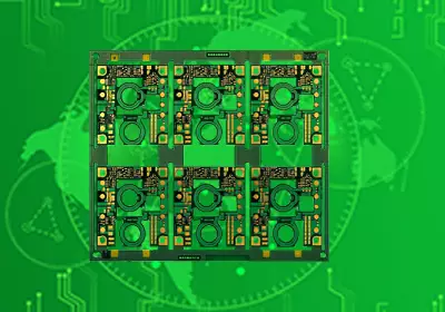
pcb board etching
The Chemistry of the Etching Process
In professional manufacturing, etching is typically divided into two distinct chemical environments, depending on whether the board is an inner layer or a fully plated outer layer. Acidic etching, often using Cupric Chloride (CuCl2), is the preferred choice for inner layers. It offers a stable etching rate and is easier to regenerate, making it highly cost-effective for high-volume production. For outer layers, where a metallic resist (like tin) protects the intended traces, an Alkaline (Ammoniacal) system is required. The alkaline chemistry is aggressive enough to dissolve the exposed copper without attacking the tin plating. Understanding these chemical dynamics is the first step in optimizing the PCB board etching line for maximum yield and consistent trace geometry.
Managing the Etch Factor and Undercut
One of the most persistent challenges for any CAM engineer is the phenomenon of "Undercut." As the chemical etchant moves vertically to remove copper, it also attacks the copper horizontally beneath the protective dry film or tin resist. This creates a trapezoidal cross-section rather than a perfect rectangle.
To compensate for this, engineers apply an "Etch Compensation" to the digital design files, making the traces slightly wider on the film than the final required width on the board. This ratio of vertical etching depth to lateral undercut is known as the Etch Factor. In high-frequency designs, where impedance must be controlled within ±5%, a consistent Etch Factor is paramount. If the PCB board etching process is not strictly controlled, the resulting narrow trace tops can lead to impedance mismatches and signal reflections, compromising the performance of the entire system.
Key Challenges in Fine Pitch Designs
As the industry moves toward HDI (High-Density Interconnect) designs with trace widths below 75\mum, the physics of fluid dynamics comes into play. A common issue in conveyor-based etching machines is the "Puddle Effect." When etchant is sprayed onto the top surface of a horizontal board, the liquid can accumulate in the center, creating a puddle that shields the copper beneath from fresh chemicals.
This leads to uneven etching across the panel, where the edges are over-etched, and the center is under-etched. Advanced PCB board etching lines solve this through intermittent spraying, oscillating nozzles, and vacuum-assisted etching systems. These technologies ensure that fresh etchant reaches every square millimeter of the copper surface uniformly, allowing for the ultra-fine lines required by modern smartphones and high-performance computing modules.
Quality Control and Environmental Considerations
The final stage of the etching process is rigorous verification. Automated Optical Inspection (AOI) scans the etched panel against the original CAD data to identify defects such as "Shorts" (excess copper) or "Opens" (over-etched gaps). Even a tiny "mouse bite" on a trace can create a localized hot spot or a signal integrity failure.
Furthermore, modern etching is increasingly focused on sustainability. Historically, etching was a waste-heavy process. Today, "closed-loop" systems allow manufacturers to regenerate the etchant on-site. By extracting the dissolved copper as high-purity copper sulfate or metallic copper through electrolysis, factories can significantly reduce chemical consumption and environmental impact, proving that high-precision manufacturing and ecological responsibility can go hand in hand.
Conclusion
Precision in the etching room is what separates a world-class PCB from a failure-prone prototype. As we look toward the future of 6G and advanced AI hardware, the demands on trace accuracy and dielectric consistency will only intensify. The PCB board etching process remains the most critical bridge between a designer’s vision and a functioning physical product. By mastering chemical balance, compensating for physical undercut, and utilizing advanced fluid control, manufacturers can deliver the high-density, low-loss circuitry that drives modern innovation. In the end, the reliability of the global electronic infrastructure is built on the precision of the lines we etch today.