A Trustworthy PCB and Electronic Manufacturing Enterprise! Contact Us



Modern laptops, tablets, and desktop workstations continue to grow sleeker, but this minimalist physical trend often leaves users with too few expansion ports. To connect high-speed external storage, mice, keyboards, displays, and network adapters simultaneously, hardware relies on multi-port USB expansion architectures. At the heart of every reliable splitter or docking station lies a central connection system that manages high-frequency data streams and power distribution seamlessly. Designing a high-performance USB hub PCB board requires strict adherence to high-speed differential signal layout rules, intelligent power management logic, and robust electrostatic discharge protection to ensure uninterrupted plug-and-play connectivity.
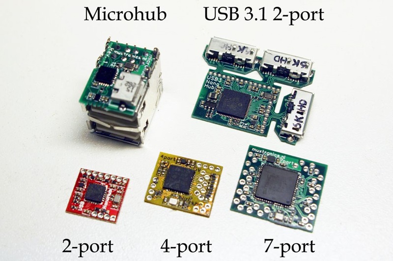
USB hub PCB board
Core Controller IC and Circuit Architecture
The brain of any USB expansion hardware is its master hub controller IC, which negotiates data transactions between the upstream host computer and multiple downstream peripheral devices.
When selecting a controller chipset, engineers must evaluate target speed standards and power budgets. Standard designs support USB 2.0 speeds (480 Mbps), while modern high-speed designs deliver USB 3.2 Gen 2 (10 Gbps) or USB4 (40 Gbps) throughput. The controller chip splits single upstream data lanes into multiple downstream channels through internal packet switching engines. Beyond basic data routing, the controller IC monitors port connection status, manages device enumeration, and regulates power delivery across each physical port.
High-Speed Signal Routing and Impedance Matching
Data integrity is the biggest challenge when routing multi-gigahertz data buses across a USB hub PCB board. At high data rates, copper traces act as transmission lines where small physical discontinuities cause severe signal reflection and bit errors.
---90Ω Differential Impedance: USB high-speed lines transmit data via differential trace pairs (D+/D- or TX+/TX- and RX+/RX-). Layout designers must maintain a strict 90Ω differential impedance (50Ω single-ended) across the entire trace path.
---Trace Length Matching: Differential signal lines in a pair must maintain identical physical lengths. Any length skew creates phase mismatch, converting clean differential signals into common-mode noise.
---Minimizing Layer Transitions: High-speed traces should remain on a single outer layer with a solid, continuous ground reference plane directly beneath them. Avoid changing layers with vias, as each via adds parasitic capacitance and inductance that disrupts high-frequency signals.
Power Management and USB Power Delivery Integration
Providing reliable power is just as critical as routing fast data lines. Expansion hubs generally operate in two power modes: Bus-Powered (drawing all electrical current from the host laptop) or Self-Powered (using an external AC/DC wall adapter).
In advanced USB-C docking hubs, integrating a dedicated Power Delivery (PD) controller allows bidirectional power negotiation. This enables pass-through charging up to 100W or higher to charge the host laptop while powering hungry downstream peripherals like external hard drives. Layout designers must place dedicated power switch ICs, low-dropout regulators (LDOs), and self-resetting polymer fuses (PPTCs) on every downstream VBUS line to prevent overcurrent damage during thermal overloads or short circuits.
Circuit Protection, ESD, and EMI Design Best Practices
Because USB ports are constantly touched by human hands and exposed to hot-plugging events, every USB hub PCB board must incorporate aggressive circuit protection against electrostatic discharge (ESD) and electromagnetic interference (EMI).
---ESD Suppression: Fast Transient Voltage Suppressor (TVS) diode arrays should be positioned as physically close to the USB connector pins as possible. These TVS components clamp voltage spikes (often exceeding several thousand volts) safely down to ground before high-voltage ESD arcs reach the main controller IC.
---EMI Filtering: Placing common-mode chokes directly on high-speed differential data lines filters out unwanted electromagnetic noise generated by fast-switching clocks.
---Grounding Strategy: Maintain a continuous, low-impedance ground plane across the middle layers. Physically isolate the noisy power ground from delicate signal ground paths, tying them together at a single clean point near the power input.
Conclusion
Creating a reliable, high-speed connectivity hardware platform requires combining high-frequency PCB routing theory with robust thermal and power safety controls. From maintaining 90Ω differential impedance matching and routing clean ground reference planes to embedding TVS protection and smart power switches, every layout decision dictates overall device stability and data transfer speeds. Partnering with a professional PCB fabrication facility that specializes in tight impedance tolerances and micro-assembly standards guarantees that your custom USB hub PCB board delivers crisp, high-speed data expansion across years of heavy daily use. By strictly controlling signal integrity and circuit protection parameters, your engineering team can build durable expansion products ready for modern digital workflows.